
Display panel and display device

A display panel and display area technology, applied in the direction of electrical components, electrical solid devices, circuits, etc., can solve problems such as difficult to meet the light input requirements of cameras, and achieve the effect of improving light transmittance and yield

Active Publication Date: 2022-04-01
WUHAN CHINA STAR OPTOELECTRONICS SEMICON DISPLAY TECH CO LTD
View PDF12 Cites 0 Cited by
  • Summary
  • Abstract
  • Description
  • Claims
  • Application Information

AI Technical Summary

Problems solved by technology

For the metal thin-layer cathode, the light transmittance of the cathode can be improved to a certain extent by reducing its thickness, but it is still difficult to meet the light input requirements of the camera

Method used


Image

  • Display panel and display device
  • Display panel and display device
  • Display panel and display device

Examples


Embodiment Construction

[0051] The following will clearly and completely describe the technical solutions in the embodiments of the present invention with reference to the drawings in the embodiments of the present invention. Apparently, the described embodiments are only some of the embodiments of the present invention, but not all of them. Based on the embodiments of the present invention, all other embodiments obtained by those skilled in the art without creative efforts fall within the protection scope of the present invention.

[0052]The following disclosure provides many different embodiments or examples for implementing different structures of the present invention. To simplify the disclosure of the present invention, components and arrangements of specific examples are described below. Of course, they are only examples and are not intended to limit the invention. Furthermore, the present disclosure may repeat reference numerals and / or reference letters in different instances, such repetiti...


PUM

PropertyMeasurementUnit
transmittivityaaaaaaaaaa

Abstract

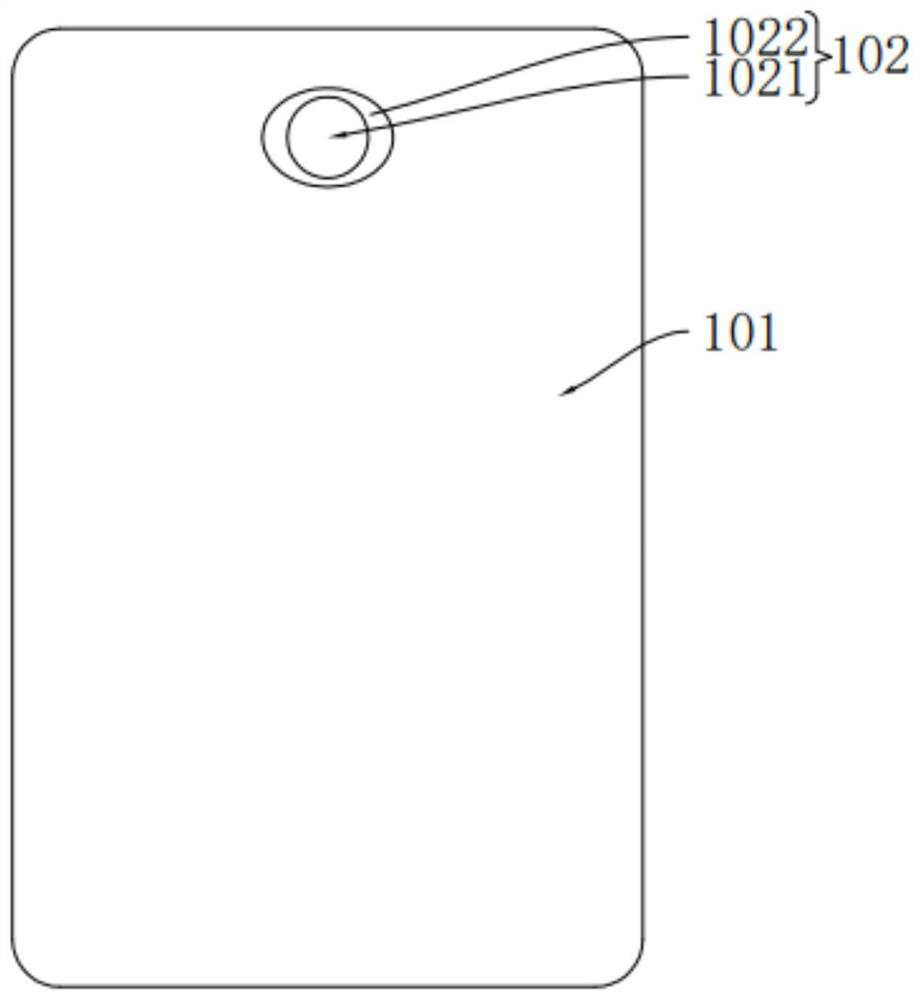
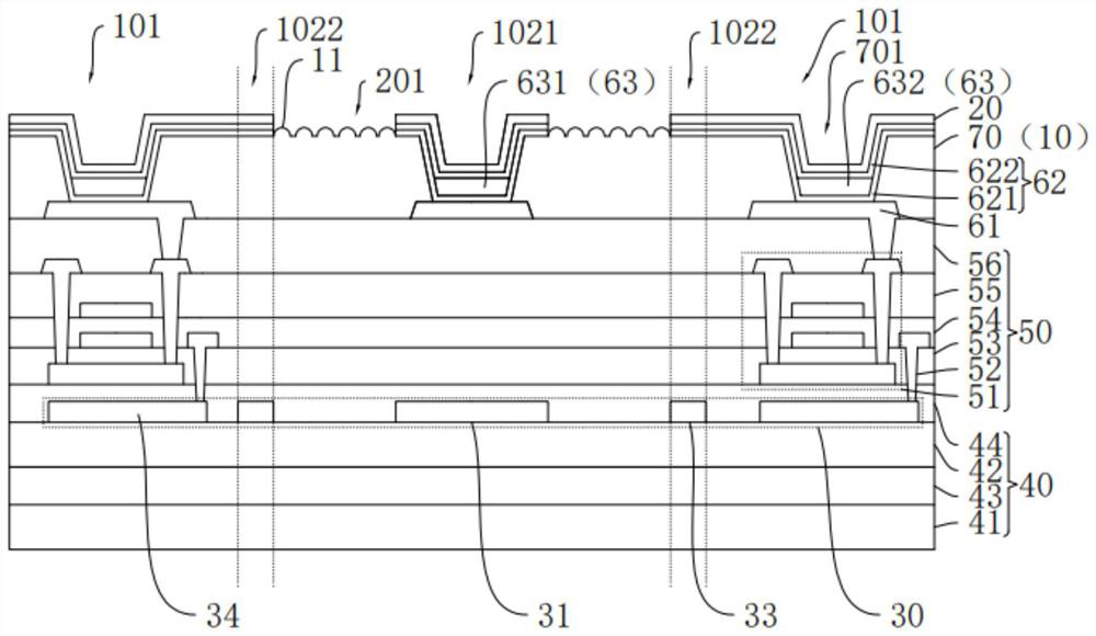
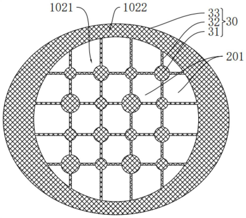
The invention discloses a display panel and a display device. The display panel comprises a conventional display area and a function display area adjacent to the conventional display area, and further comprises a driving circuit layer, a first electrode layer, a light-emitting layer and a second electrode layer. The first electrode layer is arranged in the driving circuit layer; the light-emitting layer is arranged on one side of the driving circuit layer, and the light-emitting layer comprises first light-emitting pixels arranged in the function display area and second light-emitting pixels arranged in the conventional display area; the second electrode layer is arranged on the side, away from the driving circuit layer, of the light-emitting layer, and the second electrode layer is provided with light-transmitting openings located between the adjacent first light-emitting pixels in the function display area; wherein a concave-convex structure is arranged on one side, facing the second electrode layer, of the driving circuit layer corresponding to the position of the light-transmitting opening. The light transmittance in the function display area can be improved, the stress borne by the second electrode layer during patterning is reduced, and the yield of the second electrode layer is improved.

Description

technical field [0001] The present invention relates to the field of display technology, in particular to a display panel and a display device with the display panel. Background technique [0002] As consumers' demand for screen-to-body ratio increases, under-display camera-type Organic Light-Emitting Diode (OLED) display panels have become one of the mainstream design solutions in the field of OLED display panels. [0003] For the under-screen camera, it is necessary to ensure that each film layer in the light-transmitting area directly above the camera has sufficient light transmittance. In a traditional top-emitting OLED display panel, considering the electron injection barrier, the cathode layer is usually made of a semi-transparent metal thin layer, such as Mg-Ag alloy. For the metal thin-layer cathode, the light transmittance of the cathode can be improved to a certain extent by reducing its thickness, but it is still difficult to meet the light input requirements of ...

Claims


Application Information

Patent Timeline
Patent Type & Authority Applications(China)
IPC IPC(8): H01L27/12H01L27/32
CPCH01L27/12
Inventor 金蒙吕磊杨林
Owner WUHAN CHINA STAR OPTOELECTRONICS SEMICON DISPLAY TECH CO LTD
Learn More