Semiconductor chip fine tuning test device

A test device, semiconductor technology, applied in the direction of electronic circuit testing, etc., can solve problems such as easy to shift, chips are not relatively fixed, etc.

Pending Publication Date: 2022-04-05
董玉贵
View PDF0 Cites 0 Cited by
  • Summary
  • Abstract
  • Description
  • Claims
  • Application Information

AI Technical Summary

Problems solved by technology

[0004] The purpose of the present invention is to provide a semiconductor chip fine-tuning testing device to solve the problem that the chip is not relatively fixed in the above-mentioned background technology, making it easy to shift

Method used


Image

  • Semiconductor chip fine tuning test device
  • Semiconductor chip fine tuning test device
  • Semiconductor chip fine tuning test device

Examples


Embodiment Construction

[0031] The following will clearly and completely describe the technical solutions in the embodiments of the present invention with reference to the accompanying drawings in the embodiments of the present invention. Obviously, the described embodiments are only some, not all, embodiments of the present invention. Based on the embodiments of the present invention, all other embodiments obtained by persons of ordinary skill in the art without making creative efforts belong to the protection scope of the present invention.

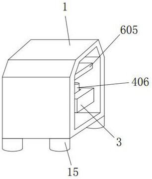
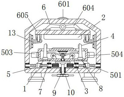
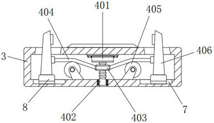
[0032] see Figure 1-6 , the present invention provides a technical solution: a semiconductor chip fine-tuning test device, including a housing 1, the front end of the housing 1 is designed to be open, the bottom four corners of the housing 1 are equipped with a base 15, the top of the inner cavity of the housing 1 There is a main body 2, the main body 2 is a test board for testing chips, the user can choose the model of the main body 2 according to actual nee...


PUM


Abstract

A semiconductor chip fine tuning test device disclosed by the present invention comprises a shell, an inner cavity of a box body is provided with a fixing mechanism, the fixing mechanism comprises a first motor, a first screw rod, a first threaded sleeve, a belt, grooved wheels and a clamping rod, the bottoms of the two grooved wheels are rotatably connected to the two sides of the bottom of the inner cavity of the box body through bearing pedestals respectively, and the clamping rod is connected with the first motor. And clamping rods are fixedly connected to one ends of the two belts correspondingly, and the outer walls of the two clamping rods are slidably connected with the openings in the two sides of the top of the box body correspondingly. According to the semiconductor chip fine tuning test device, through cooperation of a first motor, a first screw rod, a first threaded sleeve, belts, grooved wheels, clamping rods, a through groove and a block body, when the device is used, the two belts can respectively drive the two clamping rods to oppositely move left and right, and through sliding connection of the through groove and the block body, the clamping rods can move left and right; therefore, the two clamping rods can stably clamp and fix the chip, and the problem that the chip is not relatively fixed and is easy to deviate is solved.

Description

technical field [0001] The invention relates to the technical field of semiconductor chip trimming and testing, in particular to a semiconductor chip trimming and testing device. Background technique [0002] At present, in semiconductor chip testing, the testing machine needs to press the chip into the groove of the socket on the PCB test board, so that the contacts on the chip are connected to the pins of the socket, and the pins on the socket are connected to the contacts of the PCB circuit board. When the path is formed, then input a certain voltage on the PCB test board to check the output. Different voltages will produce different paths and then have different outputs. If the output matches the required parameters, it is a good product. [0003] At present, when testing semiconductors, most of the staff place the semiconductors on the workbench for manual docking. First of all, the chip is not relatively fixed, which makes it easy to shift, and the manual docking metho...

Claims


Application Information

Patent Timeline
Patent Type & Authority Applications(China)
IPC IPC(8): G01R31/28
Inventor 不公告发明人
Owner 董玉贵
Why Eureka
Try Eureka