Supercharge Your Innovation With Domain-Expert AI Agents!

Semiconductor structure

一种半导体、栅极结构的技术,应用在半导体器件、半导体/固态器件制造、电气元件等方向,能够解决金属易扩散至栅极结构等问题,达到改善金属扩散至栅极结构、增加距离、提高器件性能的效果

Pending Publication Date: 2022-04-15
FUJIAN JINHUA INTEGRATED CIRCUIT CO LTD
View PDF0 Cites 0 Cited by
  • Summary
  • Abstract
  • Description
  • Claims
  • Application Information

AI Technical Summary

Problems solved by technology

[0004] The purpose of the present invention is to provide a semiconductor structure to solve the problem that the metal in the metal silicide layer is easy to diffuse to the gate structure

Method used


Image

  • Semiconductor structure
  • Semiconductor structure
  • Semiconductor structure

Examples


Embodiment Construction

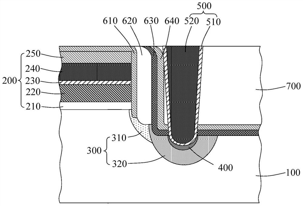
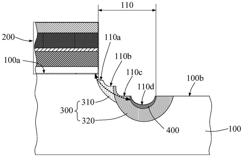
[0052] The semiconductor structure proposed by the present invention and its formation method will be further described in detail below in conjunction with the accompanying drawings and specific embodiments. The advantages and features of the present invention will become clearer from the following description. It should be noted that all the drawings are in a very simplified form and use imprecise scales, and are only used to facilitate and clearly assist the purpose of illustrating the embodiments of the present invention.

[0053] Figure 2a is a schematic diagram of a semiconductor structure in an embodiment of the present invention, Figure 2b It is a semiconductor structure in an embodiment of the present invention, which mainly shows a structural schematic diagram of a substrate.

[0054] combine Figure 2a and Figure 2b As shown, the semiconductor structure in this embodiment includes: a substrate 100 ; a gate structure 200 formed on the top surface of the substra...


PUM


Abstract

The invention provides a semiconductor structure. At least two isolation side walls of which the bottoms are sequentially lowered are arranged on the side edge of a gate structure, and the bottom of a contact plug is further lowered to extend into a substrate, so that a metal silicide layer is sunken in a deeper position of the substrate, and the distance between the metal silicide layer and the gate structure is increased. Therefore, the problem that metal is diffused to the gate structure in the preparation process of the metal silicide layer and after the preparation of the metal silicide layer is completed can be effectively improved.

Description

technical field [0001] The invention relates to the technical field of semiconductors, in particular to a semiconductor structure. Background technique [0002] Transistor devices, as the main devices in semiconductor integrated circuits, are widely used in memory and logic circuits. specific reference figure 1 As shown, the transistor generally includes a gate structure 20 formed on the surface of the substrate 10 and a source-drain region 30 formed in the substrate 10 and located on the side of the gate structure 20, wherein the source-drain region 30 usually also needs The electrical extraction is realized through the contact plug 50 , that is, the bottom of the contact plug 50 extends to the substrate 10 to be electrically connected to the source and drain regions 30 . [0003] In the prior art, in order to reduce the contact resistance between the contact plug 50 and the source-drain region 30, a metal silicide layer 40 is generally formed on the contact surface of th...

Claims


Application Information

Patent Timeline
Patent Type & Authority Applications(China)
IPC IPC(8): H01L21/8234H01L21/768H01L29/78H01L21/336
CPCH01L29/78H01L29/665H01L21/76897
Inventor 颜逸飞朱家仪
Owner FUJIAN JINHUA INTEGRATED CIRCUIT CO LTD
Features
  • R&D
  • Intellectual Property
  • Life Sciences
  • Materials
  • Tech Scout
  • Unparalleled Data Quality
  • Higher Quality Content
  • 60% Fewer Hallucinations
Learn More