
TFT structure of multiplex circuit, display panel and display device

A technology of multiplexing circuits and metal layers, which is applied in the direction of circuits, electrical components, electric solid devices, etc., can solve the problems of TFT structure positive bias, affecting the driving function of multiplexing circuits, etc., and achieve the effect of improving driving performance

Pending Publication Date: 2022-04-15
广州华星光电半导体显示技术有限公司
View PDF0 Cites 0 Cited by
  • Summary
  • Abstract
  • Description
  • Claims
  • Application Information

AI Technical Summary

Problems solved by technology

[0004] Based on this, it is necessary to solve the problem that the TFT structure at the multiplexing circuit on the existing display panel is turned on multiple times in a short period of time, so that the TFT structure at the multiplexing circuit is severely forward-biased and affects the driving function of the multiplexing circuit. TFT structure of a multiplexing circuit, display panel and display device

Method used


Image

  • TFT structure of multiplex circuit, display panel and display device
  • TFT structure of multiplex circuit, display panel and display device
  • TFT structure of multiplex circuit, display panel and display device

Examples


Embodiment Construction

[0033] In order to facilitate the understanding of the present application, the present application will be described more fully below with reference to the relevant drawings. A preferred embodiment of the application is shown in the drawings. However, the present application can be embodied in many different forms and is not limited to the embodiments described herein. On the contrary, the purpose of providing these embodiments is to make the disclosure of this application more thorough and comprehensive.

[0034] It should be noted that when an element is considered to be "connected" to another element, it may be directly connected to and integrally integrated with the other element, or there may be an intervening element at the same time. The terms "stack", "one side", "other side" and similar expressions are used herein for the purpose of description only. In addition, the serial numbers such as "first" and "second" mentioned in this application do not represent any sequ...


PUM


Abstract

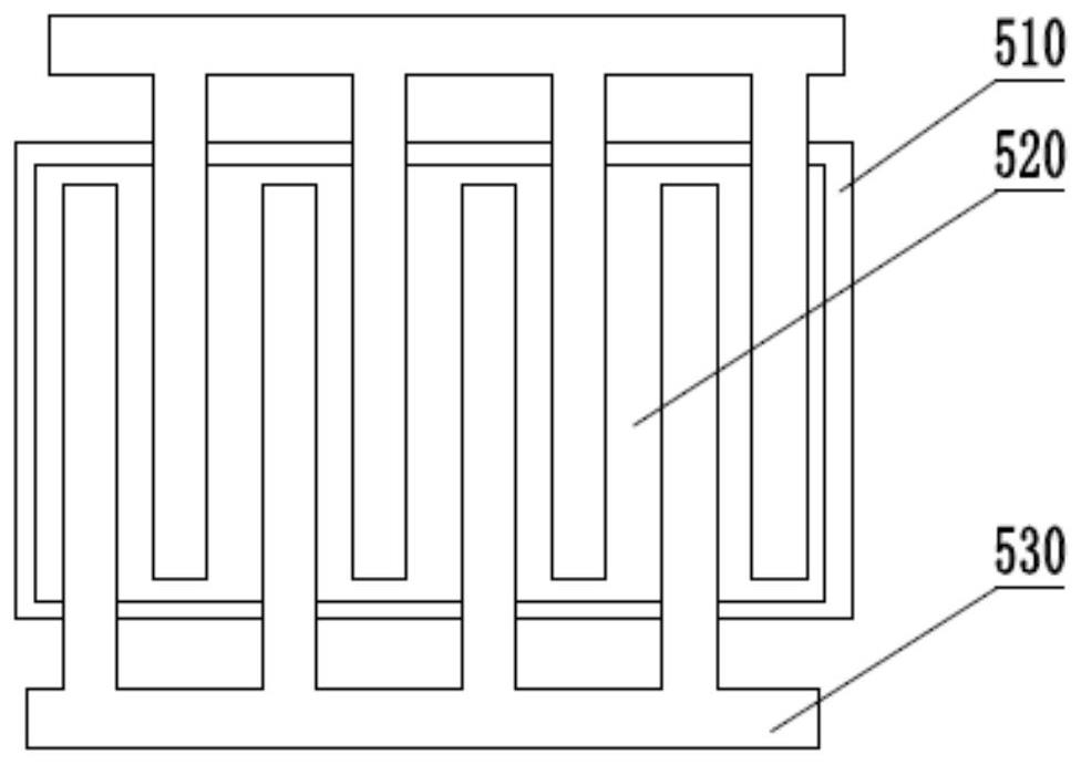
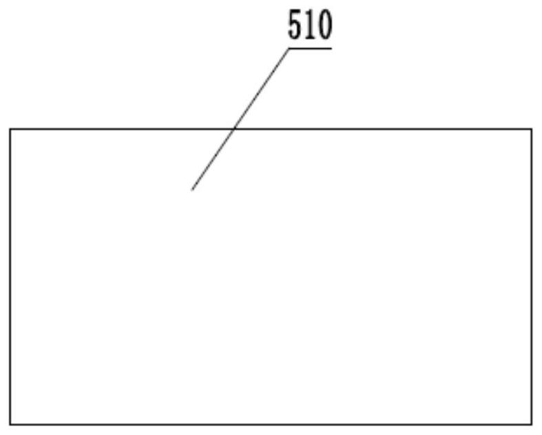
The invention relates to a TFT structure of a multiplex circuit, a display panel and a display device. The TFT structure of the multiplexing circuit comprises a first active layer and a first metal layer, wherein the first metal layer and the first active layer are sequentially arranged along the direction of backlight rays; the first metal layer is provided with a first backlight channel, and the backlight rays penetrate through the first backlight channel to irradiate the first active layer. The first metal layer is provided with the first backlight channel, so that backlight rays can irradiate on the first active layer through the first backlight channel, and the backlight rays irradiate on the first active layer to increase carriers on the first active layer, thereby causing Vth negative bias of the TFT structure of the multiplexing circuit; the Vth negative bias part of the TFT structure of the multiplexing circuit counteracts the Vth positive bias of the TFT structure of the multiplexing circuit due to multiple times of opening in a short time, so that the driving performance of the multiplexing circuit is improved.

Description

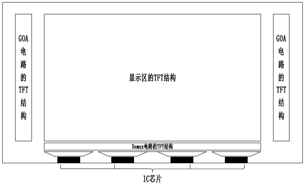
technical field [0001] The present application relates to the technical field of display devices, in particular to a TFT structure of a multiplexing circuit, a display panel and a display device. Background technique [0002] In the manufacturing process of display panels, IC chips account for a large proportion of the cost. In order to reduce the number of IC chips and reduce production costs, the signals from the IC chips on the display panel to the Gate or Data often use a Demux (multiplexing) circuit design. Existing Demux circuits such as Figure 4 As shown, the output signal D1 of the IC chip ( Figure 5 Middle Data signal) is input to the pixels in columns S1, S5, and S3 through the signal output wiring through the switches T1, T2, and T3 respectively. [0003] Taking the existing 1920*1080 display panel as an example, the display panel has 1920*3 columns of pixels, and one output signal of the IC chip can be input into three columns of pixels, so the display panel ...

Claims


Application Information

Patent Timeline
IPC IPC(8): H01L27/12
Inventor 刘倩
Owner 广州华星光电半导体显示技术有限公司
Learn More