Transistor structure and forming method thereof

A technology of transistor and electrode structure, which is applied in the direction of semiconductor devices, semiconductor/solid-state device manufacturing, electrical components, etc. It can solve the problems of large square resistance, the extension method cannot independently optimize the balance, serious problems, etc., and achieve the effect of improving driving performance

Active Publication Date: 2014-06-18
SEMICON MFG INT (SHANGHAI) CORP
View PDF3 Cites 0 Cited by
  • Summary
  • Abstract
  • Description
  • Claims
  • Application Information

AI Technical Summary

Problems solved by technology

However, in the prior art, in order to control the short channel effect, the junction depth of the source/drain extension region is generally required to be very small, resulting in an excessively large sheet resistance of the source/drain extension region
[0005] Therefore, the use of high-mobility alloy materials to reduce the sheet resistance of the source/drain extension region has become a new method. The existing method is usually to form the source/drain extension through a special lateral etching method while forming the sourc

Method used


Image

  • Transistor structure and forming method thereof
  • Transistor structure and forming method thereof
  • Transistor structure and forming method thereof

Examples


Embodiment Construction

[0043] For ease of understanding, the following combination Figure 1 to Figure 11 The present invention is further described with specific examples. Advantages and features of the present invention will be apparent from the following description and claims. It should be noted that all the drawings are in a very simplified form and use imprecise scales, and are only used to facilitate and clearly assist the purpose of illustrating the embodiments of the present invention.

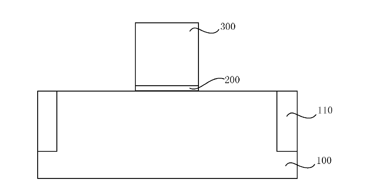
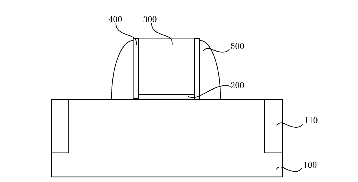
[0044] Please refer to figure 2 and image 3 , first perform step S101, providing a semiconductor substrate 100, on which a dummy gate electrode structure and a dummy spacer 500 are provided, the dummy gate electrode structure includes a dummy gate dielectric layer 200 and is formed on the dummy The dummy gate electrode 300 on the gate dielectric layer 200 , the dummy spacer 500 is formed on both sides of the dummy gate dielectric layer 200 and the dummy gate electrode 300 .

[0045] Wherein, a shallow...


PUM

PropertyMeasurementUnit
Depthaaaaaaaaaa

Abstract

The invention provides a transistor structure forming method and a transistor structure. After a source and a drain are formed, the source and the drain are etched to form depth-controllable and shape-controllable source and drain extension region grooves. Meanwhile, the short channel effect of the transistor can be controlled by carrying out depth control on the junction depth of source and drain extension regions and reducing a predetermined transistor series resistance, thus achieving the purpose of effectively improving the driving performance of the transistor.

Description

technical field [0001] The invention relates to the field of semiconductor manufacturing, in particular to a transistor structure and a forming method thereof. Background technique [0002] With the deduction of Moore's Law, the microelectronics industry is approaching the limit of smaller scale and line width. With the continuous reduction of device feature size, conventional scaling methods have encountered a series of problems centered on the short channel effect. For example, as the transistor scales further, the parasitic series resistance of the transistor increases dramatically, reducing the response speed of the entire transistor. [0003] In recent years, strain engineering (Strain Engineering) technology has been introduced to improve transistor speed. A major technique in strain engineering is transistor source / drain selective epitaxy of substrate material alloys with different crystal lattices. Among them, the main manufacturing method of this technology is: b...

Claims


Application Information

Patent Timeline
IPC IPC(8): H01L21/336H01L29/78H01L29/08
CPCH01L29/0847H01L29/66636H01L29/78
Inventor 殷华湘
Owner SEMICON MFG INT (SHANGHAI) CORP
Why Eureka
Try Eureka