Improvement method and improvement structure of driving circuit of multi-phase charge pump
A driving circuit and charge pump technology, applied in the field of microelectronics, can solve the problems of low system efficiency and high chip heating, and achieve the effects of improving system efficiency, saving power loss, and preventing Vout from being backflowed.
- Summary
- Abstract
- Description
- Claims
- Application Information
AI Technical Summary
Problems solved by technology
Method used
Image
Examples
Embodiment 1
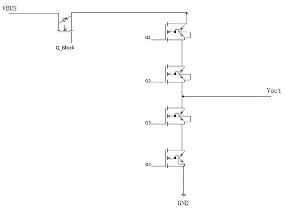
[0031] For a multi-phase charge pump, the charge pump chip is equipped with four multi-phase cascaded NMOS transistors, namely NMOS transistors Q1, Q2, Q3, and Q4; the drain of the NMOS transistor Q1 is connected to the power input terminal VBUS, and the S of the NMOS transistor Q1 The pole is connected to the D pole of the NMOS transistor Q2, the S pole of the NMOS transistor Q2 is connected to the D pole of the NMOS transistor Q3, the S pole of the NMOS transistor Q3 is connected to the D pole of the NMOS transistor Q4; the S pole of the NMOS transistor Q2 is connected to the D pole of the NMOS transistor Q3 The output terminal Vout is also connected.
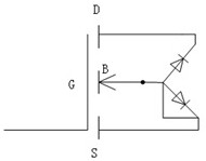
[0032] Such as Figure 4 As shown, in this embodiment, the NMOS transistor Q2 used as the primary MOS in the multi-phase cascaded MOS according to image 3 The structure, disconnect the short-circuited part of the B pole and the S pole, connect the B pole to the input terminal VBUS through a Schottky diode, and connect the B...
Embodiment 2
[0036] Embodiment 2 adopts another low-level control scheme on the basis of Embodiment 1, as follows:
[0037] For a multi-phase charge pump, the charge pump chip is equipped with four multi-phase cascaded NMOS transistors, namely NMOS transistors Q1, Q2, Q3, and Q4; the drain of the NMOS transistor Q1 is connected to the power input terminal VBUS, and the S of the NMOS transistor Q1 The pole is connected to the D pole of the NMOS transistor Q2, the S pole of the NMOS transistor Q2 is connected to the D pole of the NMOS transistor Q3, the S pole of the NMOS transistor Q3 is connected to the D pole of the NMOS transistor Q4; the S pole of the NMOS transistor Q2 is connected to the D pole of the NMOS transistor Q3 The output terminal Vout is also connected.
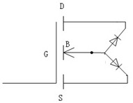
[0038] Such as Figure 5 As shown, in this embodiment, the NMOS transistor Q2 used as the primary MOS in the multi-phase cascaded MOS according to image 3 The structure, disconnect the short-circuited part of the B pole ...
PUM
 Abstract
Description
Claims
Application Information


