Phased array time-frequency synchronous distribution time delay consistency automatic calibration system
A time-frequency synchronization and consistency technology, applied in the field of phased array radar, can solve the problem of large delay calibration error
Pending Publication Date: 2022-04-22
NO 34 RES INST OF CHINA ELECTRONICS TECH GRP
0 Cites 0 Cited by
AI-Extracted Technical Summary
Problems solved by technology
[0004] The purpose of the present invention is to provide a phased array time-frequency synchronous distribution time delay consistency aut...
Abstract
The invention relates to the technical field of phased array radars, in particular to a phased array time-frequency synchronous distribution time delay consistency automatic calibration system which comprises an electro-optical unit, an optical power division unit, an operation and maintenance unit and a plurality of array element photoelectric units. The operation and maintenance unit issues instructions to the electro-optical unit, the optical power division unit and the plurality of array element photoelectric units; the photoelectric unit outputs a reference radio frequency signal and performs electro-optical conversion, and after the loopback optical signal output by the optical power division unit is converted into a loopback electric signal, the delay inequality of the reference radio frequency signal and the loopback electric signal is measured; the optical power division unit performs time delay adjustment on the output reference radio frequency optical signal, transmits an adjusted adjustment signal to the array element photoelectric unit, amplifies a reflected signal of the array element photoelectric unit, and transmits the amplified reflected signal as a loopback optical signal to the electro-optical unit; and the array element photoelectric unit reflects the adjustment signal as a reflection signal back to the optical power division unit, so that the problem of large error caused by manual adjustment in the existing time delay calibration is solved.
Application Domain
Wave based measurement systems
Technology Topic
Optical powerLoopback +6
Image
Examples
- Experimental program(1)
Example Embodiment
[0039] The following describes in detail the embodiments of the present invention, examples of which are illustrated in the accompanying drawings, wherein the same or similar reference numerals refer to the same or similar elements or elements having the same or similar functions throughout. The embodiments described below with reference to the accompanying drawings are exemplary, and are intended to explain the present invention and should not be construed as limiting the present invention.
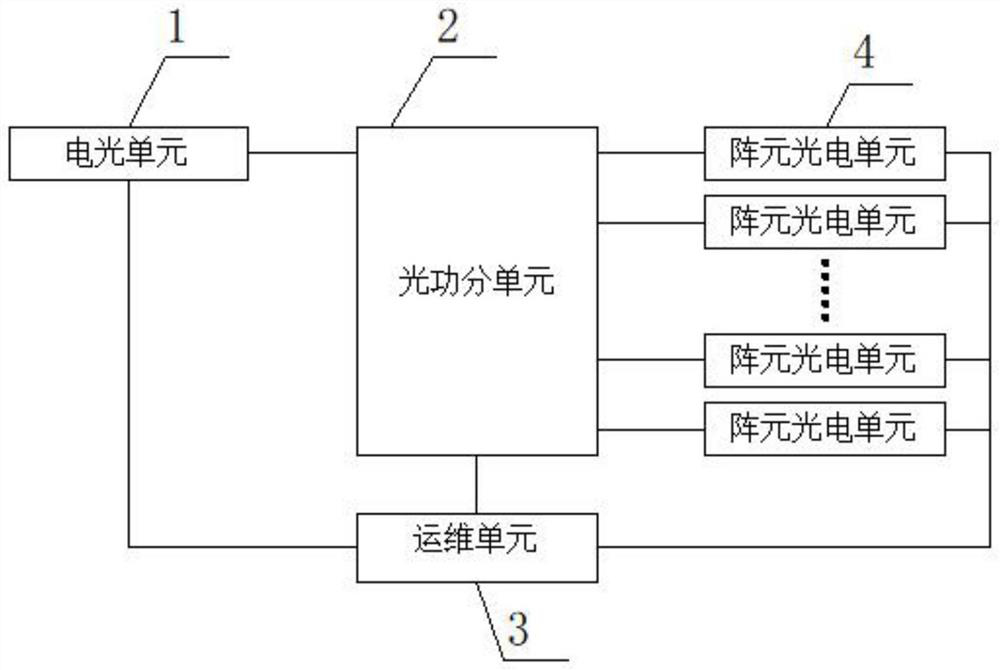
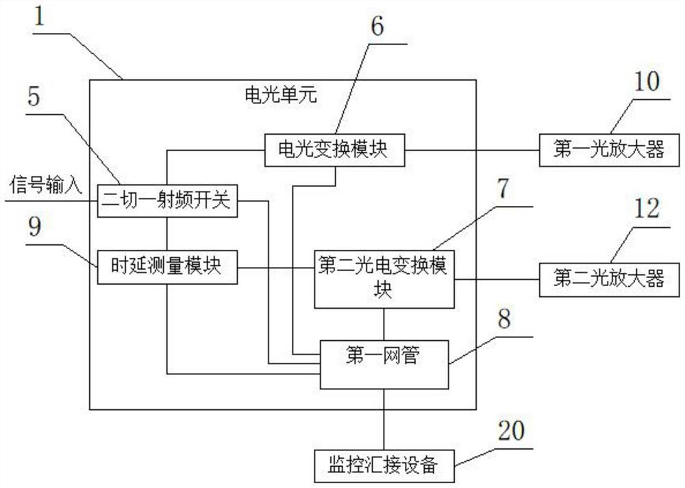
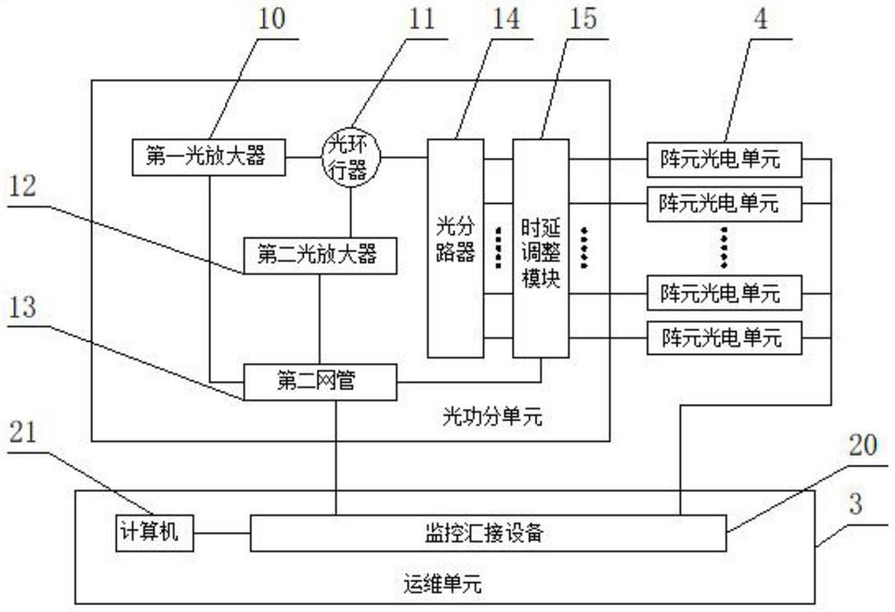
[0040] see Figure 1 to Figure 4 , the present invention provides a phased array time-frequency synchronous distribution delay consistency automatic calibration system, including an electro-optical unit 1, an optical power division unit 2, an operation and maintenance unit 3 and a plurality of array element photoelectric units 4;
[0041]The electro-optical unit 1 is connected to the optical power division unit 2, a plurality of the array element optoelectronic units 4 are respectively connected to the optical power division unit 2, and the operation and maintenance unit 3 is connected to the electro-optical unit 1 and the optical power division unit. 2 and several of the array element photoelectric units 4 are connected;
[0042] The operation and maintenance unit 3 is used to issue instructions to the electro-optical unit 1, the optical power division unit 2 and a number of the array element optoelectronic units 4;
[0043] The electro-optical unit 1 is used to output a reference radio frequency signal, convert the reference radio frequency signal into a reference radio frequency optical signal for output, and convert the loopback optical signal output by the optical power division unit 2 into a loopback electrical signal, and measure the delay difference between the reference radio frequency signal and the loopback electrical signal;
[0044] The optical power division unit 2 is used to adjust the time delay of the output reference radio frequency optical signal, and at the same time transmit the adjusted adjustment signal to the array element optoelectronic unit 4, and the array element optoelectronic unit 4 The reflected signal is amplified and transmitted to the electro-optical unit 1 as the loopback optical signal;
[0045] The array element photoelectric unit 4 is configured to reflect the adjustment signal back to the optical power division unit 2 as the reflected signal.
[0046] Specifically, when calibrating the time delay consistency of the channels, first measure the time delay value of each channel. Specifically, the electro-optical unit 1 outputs the reference radio frequency signal, and the optical power division unit 2 outputs the reference RF signal. The reference radio frequency signal in the initial unadjusted state is transmitted to the array element photoelectric unit 4, and the array element photoelectric unit 4 reflects the reflected signal of the reference radio frequency signal to the optical power division unit 2, and the The optical power division unit 2 amplifies the reflected signal and transmits it back to the electro-optical unit 1 to obtain the current delay value T 1 , and report the delay value to the operation and maintenance unit 3. After the operation and maintenance unit 3 accepts the delay value, it controls the output direction of the array element photoelectric unit 4, so as to detect the calibration Delay value T for each remaining channel in the range 2 , T 3...T N , so as to obtain the delay value T of each passing 1 , T 2 , T 3...T N , and report all data to the operation and maintenance unit 3, the operation and maintenance unit 3 selects the calibration reference channel, and marks the delay value of the calibration reference channel as T 0 , and then calculate the experimental difference T of the delay value of each channel Δ1 , T Δ2 , T Δ3...T ΔN-1 , and finally the operation and maintenance unit 3 controls the optical power division unit 2 to perform T on each pass Δ1 , T Δ2 , T Δ3...T ΔN-1 Precise adjustment of the delay difference. The measurement response time of each link is determined by the transmission time and signal processing time. The transmission time is mainly determined by the length of the optical link. For example, the transmission delay of a 200m fiber is about 1us, and the signal processing time is about Therefore, the delay measurement response time of each link should also be in the order of 100ms, and the delay measurement time of 100 channels can be kept within 10s, which can realize fast and accurate delay measurement. Since the optical delay line adopts micro-motor-controlled micro-step continuous adjustment, the conventional adjustment speed is about 40ps/s, and the delay adjustment time is proportional to |TΔ|. Since the system has the largest deviation during the first calibration after deployment, It mainly compensates for the delay difference caused by the physical length difference between each channel, and the correction range is large. The maximum difference of the fiber delay of each channel with a slightly controlled wiring length of 100m can be controlled within 500ps (10cm length fiber), so The maximum single-channel delay correction delay of the first 100m wiring magnitude is about 12.5s, and the average delay correction time is about 6s, so the first phase correction time of the hundred-channel magnitude is about 10min. The timing of delay correction in work is mainly caused by the temperature difference of the fibers of each channel. Usually, the delay difference is not too large. Calculated according to the wiring length of 100m and the temperature difference between fibers of 10°C, the maximum delay difference is 40ps. , the delay correction of one channel can be completed within 1s, so the regular work correction period of the 100m-level hundred-channel delay correction is about 100s. It solves the problem that the existing time delay calibration has a large error through manual adjustment. It also eliminates the delay error caused by the uneven temperature of the construction wiring or the use of the environment.
[0047] Further, the electro-optical unit 1 includes a two-to-one radio frequency switch 5, an electro-optical conversion module 6, a second photoelectric conversion module 7, a first network management 8 and a delay measurement module 9. The two-to-one radio frequency switch 5, the The electro-optical conversion module 6 , the first network management 8 and the delay measurement module 9 are connected in sequence, the first network management 8 is connected to the two-to-one radio frequency switch 5 , and the second photoelectric conversion module 7 is connected to the delay The measurement module 9 is connected to the first network management 8;
[0048] The first network management 8 is configured to control the two-to-one radio frequency switch 5 according to the first control instruction issued by the operation and maintenance unit 3;
[0049] The two-to-one radio frequency switch 5 controls the power-on and power-off of the second photoelectric conversion module 7 and the delay measurement module 9 based on the first control command;
[0050] The time delay measurement module 9 is configured to output a reference radio frequency signal and measure the time delay difference between the reference radio frequency signal and the loopback electrical signal;
[0051] The electro-optical conversion module 6 is used to convert the reference radio frequency signal into a reference radio frequency optical signal;
[0052] The second photoelectric conversion module 7 is used to convert the loopback optical signal into a loopback electrical signal.
[0053] Specifically, the 2-in-1 RF switch 5 has 2 RF input interfaces, 1 RF output interface, and 1 control interface, and the electro-optical conversion module 6 has 1 RF input interface, 1 optical output interface, and 1 RF input interface. Reporting interface, the second photoelectric conversion module 7 has an optical input interface, a radio frequency output interface, and a reporting control interface, and the delay measurement module 9 has a reference output interface, a loopback radio frequency input interface, 1 a reporting control interface, the first network management 8 has four internal monitoring interfaces and one external network management interface, the input interface of the time-frequency signal is the same as the radio frequency input interface of the two-to-one radio frequency switch 5, so The reference output interface of the delay measurement module 9 is connected to another radio frequency input interface of the two-to-one radio frequency switch 5, and the radio frequency output interface of the two-to-one radio frequency switch 5 is connected to the radio frequency input interface of the electro-optical conversion module 6. , the control interface of the two-to-one radio frequency switch 5 is connected to a monitoring interface of the first network management 8, the reporting interface of the second photoelectric conversion module 7 is connected to a monitoring interface of the first network management 8, The radio frequency output interface of the second photoelectric conversion module 7 is connected to the loopback radio frequency input interface of the delay measurement module 9, and the reporting control interface of the second photoelectric conversion module 7 is connected to a monitoring interface of the first network management 8, The reporting control interface of the delay measurement module 9 is connected to a monitoring port of the first network management 8 , and the first network management 8 sends an external network management interface to the operation and maintenance unit 3 .
[0054] Further, the optical power division unit 2 includes a first optical amplifier 10, an optical circulator 11, a second optical amplifier 12, a second network management system 13, an optical splitter 14 and a delay adjustment module 15. The first optical The amplifier 10, the optical circulator 11, the second optical amplifier 12 and the second network management 13 are connected in sequence, the second optical amplifier 12 is connected to the second photoelectric conversion module 7, and the optical branch The optical circulator 14 is connected to the optical circulator 11, and the delay adjustment module 15 is connected to the optical splitter 14;
[0055] The second network management 13 is used to receive the adjustment instruction and the third control instruction issued by the operation and maintenance unit 3, and transmit the adjustment instruction to the delay adjustment module 15, and based on the third control The instruction controls the power-on and power-off of the second optical amplifier 12;
[0056] The first optical amplifier 10 is used to amplify the power of the reference radio frequency optical signal to obtain an amplified signal;
[0057] The optical circulator 11 is used to transmit the amplified signal to the optical splitter 14, and transmit the reflected signal reflected by the array element photoelectric unit 4 to the second optical amplifier 12;
[0058] The optical splitter 14 is used to divide the amplified signal into several split signals and transmit them to the delay adjustment module 15;
[0059] The delay adjustment module 15 adjusts the delay amounts of several of the branched signals based on the adjustment instruction to obtain several adjusted optical signals;
[0060] The second optical amplifier 12 is used to amplify the reflected signal and transmit it to the second photoelectric conversion module 7 as the loopback optical signal.
[0061] Specifically, the first optical amplifier 10 has one optical input interface, one optical output interface, and one reporting control interface, and the optical circulator 11 has three ports, which are the first optical port, the second optical port, the first optical port, and the third optical port. Three optical ports, the second optical amplifier 12 has an optical input interface, an optical output interface, and a reporting control interface, and the optical splitter 14 has an optical input interface and several optical output interfaces, The channel delay adjustment module 15 mainly has several optical input interfaces and several optical output interfaces, and the second network management 13 has three internal monitoring interfaces, one external network management interface and one reporting control interface. The optical output interface of the electro-optical conversion module 6 is connected to the optical input interface of the first optical amplifier 10, the reporting control interface of the first optical amplifier 10, the monitoring interface of the second network management 13, the optical circulator 11 The first optical port of the optical circulator 11 is connected to the optical output port of the first optical amplifier 10, the second optical port of the optical circulator 11 is connected to the optical input port of the optical splitter 14, and the second optical port of the optical circulator 11 is connected to the optical input port of the optical splitter 14. The three optical ports are connected to the input optical port of the second optical amplifier 12 , the reporting control port of the second optical amplifier 12 is connected to one monitoring port of the second network management 13 , and the optical port of the second optical amplifier 12 The output interfaces are connected to the optical input interfaces of the second photoelectric conversion module 7, and the optical output interfaces of the optical splitter 14 are respectively connected to the optical input interfaces of the channel delay adjustment module 15 through short fiber jumpers. , the reporting control interface of the channel delay adjustment module 15 is connected to a monitoring interface of the second network management 13, and its main function is to accept the delay adjustment information issued by the second network management 13, and adjust the delay amount on the specified path. , the core of the delay adjustment module 15 is a continuous dimmable delay line driven by a micro-motor based on several internal channels, the delay adjustment accuracy is higher than 1ps, and the total delay range is determined according to the correction deviation capacity, which can be An optical delay line with a suitable range is selected in 100ps-5ns; the external network management interface of the second network management 13 is connected to the operation and maintenance unit 3 .
[0062] Further, the array element photoelectric unit 4 includes all two optical switches 16, a light reflector 17, a first photoelectric conversion module 18 and a third network management 19, the all two optical switches 16, the first photoelectric conversion module 18 Connected to the third network management 19 in turn, and the light reflector 17 is connected to the all two optical switches 16;
[0063] The third network management 19 is used to control all the two optical switches 16 according to the second control instruction issued by the operation and maintenance unit 3;
[0064] The all two optical switches 16 are used to control the power-on and power-off of the light mirror 17 and the first photoelectric conversion module 18 based on the second control instruction;
[0065] The first photoelectric conversion module 18 is configured to convert the corresponding adjusted optical signal into an adjusted electrical signal and output it;
[0066] The optical mirror 17 is used to totally reflect the reflected signal of the corresponding adjusted optical signal to the optical circulator 11 via the delay adjustment module 15 and the optical splitter 14 .
[0067]Specifically, the all two optical switches 16 have one input optical port, two output optical ports, and one control interface, and the first photoelectric conversion module 18 has one optical input interface, one radio frequency output interface, and one radio frequency output interface. There are two reporting control interfaces, the optical mirror 17 has only one optical interface, the third network management system 19 has two monitoring interfaces and one external network management interface, and the input optical interfaces of all the two optical switches 16 are connected to the channel delay Several optical output ports of the adjustment module 15 and their corresponding optical output ports, the two output ports of the all-two optical switches 16 are respectively connected to the optical ports of the light reflector 17 and the optical ports of the first photoelectric conversion module 18 . The optical input interface and the control interface of all two optical switches 16 are connected to a monitoring interface of the third network management 19, and the radio frequency output interface of the first photoelectric conversion module 18 is the output interface of the adjustment signal, so the The reporting control interface of all the two optical switches 16 is connected to a monitoring interface of the third network management system 19 , and some external network management interfaces of the third network management system 19 are connected to the operation and maintenance unit 3 .
[0068] Further, the operation and maintenance unit 3 includes a monitoring tandem device 20 and a computer 21 , and the monitoring tandem device 20 is connected to the first network management 8 , the second network management 13 and the third network management 19 . The computer 21 is connected to the monitoring tandem device 20;
[0069] The computer 21 is used to input the first control instruction, the second control instruction and the adjustment instruction to the monitoring tandem device 20;
[0070] The monitoring tandem device 20 is configured to issue the first control instruction to the first network management 8, issue the second control instruction to the third network management 19, and send the adjustment instruction and the The third control instruction is issued to the second network management 13 .
[0071] Specifically, the monitoring tandem device 20 has several +2 monitoring interfaces and interactive interfaces, which are respectively connected to the external network management interfaces of the third network management 19 and the first network management 8 of the array element photoelectric units 4 . The external network management interface of the second network management system 13 and the external network management interface of the second network management device 13 , and the interactive interface of the monitoring tandem device 20 is connected to the computer 21 .
[0072] When calibrating the delay consistency, the monitoring tandem device 20 issues the first control instruction through the first network management 8, and the two-in-one radio frequency switch 5 controls the The time delay measurement module 9 and the electro-optical conversion module 6 are powered on, and the radio frequency input interface of the two-to-one radio frequency switch 5 connected to the input interface of the time-frequency signal is controlled to be disconnected, and the monitoring tandem equipment 20 Issue the third control command through the second network management 13 to control the second optical amplifier 12 to be powered on, the delay adjustment module 15 is in a delay maintaining state, and the third network management 19 controls the The all-two optical switch 16 is switched to the optical mirror 17, the time delay measurement module 9 outputs a reference radio frequency signal, the electro-optical conversion module 6 converts the reference radio frequency signal into the reference radio frequency optical signal, the The first optical amplification signal converts the reference radio frequency optical signal into an electrical signal, and is output from the first optical port of the optical circulator 11 through the second optical port to the optical splitter 14 after the delay adjustment The module 15 is sent to the optical mirror 17, and the optical mirror 17 totally reflects the reference radio frequency optical signal as a reflected signal to the optical ring through the delay adjustment module 15 and the optical splitter 14. The second optical port of the optical device 11 is sent to the second optical amplifier 12 through the third optical port. The second optical amplifier 12 amplifies the reflected signal and transmits it to the second photoelectric converter as a loopback optical signal. Module 7, the second photoelectric conversion module 7 converts the loopback optical signal into a loopback electrical signal, and the delay measurement module 9 measures the delay value T of the current channel based on the loopback electrical signal 1 , and report the delay value to the monitoring tandem device 20 of the operation and maintenance unit 3 through the first network management After sending the second adjustment command, the two optical switches 16 switch to the first photoelectric conversion module 18 based on the second adjustment command until the delay measurement of the current link is completed, and then the monitoring and tandem connection is performed. The device 20 automatically controls the output direction of all the two optical switches 16 inside the array element photoelectric unit 4 in the selected channel, so as to measure the delay value T of each remaining channel within the calibration range. 2 , T 3...T N , the monitoring tandem device 20 of the operation and maintenance unit 3 selects a calibration reference channel, and marks the time delay value of the calibration reference channel as T 0 , and then calculate the experimental difference T of the delay value of each channel Δ1 , T Δ2 , T Δ3...T ΔN-1 , and finally the monitoring tandem device 20 of the operation and maintenance unit 3 sends the adjustment instruction to the delay adjustment module 15 through the second network management system 13, and the delay adjustment module 15 is based on the adjustment instruction T for each pass Δ1 , T Δ2 , T Δ 3...T ΔN-1 Precise adjustment of delay difference.
[0073] When transmitting the signal, the monitoring tandem device 20 issues the first control command through the first network management 8, and the two-to-one radio frequency switch 5 converts the time-frequency switch 5 based on the first control command The input interface of the signal is communicated with the electro-optical conversion module 6, and controls the delay measurement module 9 and the second photoelectrical conversion module 7 to be powered off, and the monitoring tandem device 20 sends a third signal to the second network management 13. control command, the second network management 13 controls the second optical amplifier 12 to power off based on the third control command, and the monitoring tandem device 20 issues the second control command through the third network management 19, The all-two optical switches 16 are switched to the first photoelectric conversion module 18 based on the second control command. After the output time-frequency signal is converted into a second optical signal by the electro-optical conversion module 6, the first optical signal is converted into a second optical signal. An optical amplifier 10 amplifies the second optical signal, and the amplified second amplified signal is output to the optical splitter 14 through the first optical port of the optical circulator 11 through the second optical port. The optical splitter 14 divides the second amplified signal into a plurality of second split signals and outputs them to the delay adjustment module 15. The delay adjustment module 15 includes several channels of reconfigurable optical delays. line, the state of the delay adjustment module 15 in the delay maintaining state is maintained in the state after the last adjustment, and a number of the second branch signals pass through a number of optical fiber output values of all the array element photoelectric units 4. The first photoelectric conversion module 18, the first photoelectric conversion module 18 converts the corresponding second branch signal into an electrical signal and outputs it.
[0074] The above disclosure is only a preferred embodiment of a phased array time-frequency synchronization distribution delay consistency automatic calibration system of the present invention, of course, it cannot limit the scope of rights of the present invention, and those of ordinary skill in the art can understand All or part of the flow of the above-mentioned embodiments, and equivalent changes made according to the claims of the present invention, still belong to the scope covered by the present invention.
PUM


Description & Claims & Application Information
We can also present the details of the Description, Claims and Application information to help users get a comprehensive understanding of the technical details of the patent, such as background art, summary of invention, brief description of drawings, description of embodiments, and other original content. On the other hand, users can also determine the specific scope of protection of the technology through the list of claims; as well as understand the changes in the life cycle of the technology with the presentation of the patent timeline. Login to view more.