PCB defect detection method based on re-verification detection

A PCB board and defect detection technology, applied in image analysis, image enhancement, instruments, etc., can solve problems such as PCB board defect detection, and achieve the effect of preventing overfitting and achieving effective expansion.

Pending Publication Date: 2022-04-22
UNIV OF SCI & TECH BEIJING
View PDF0 Cites 2 Cited by
  • Summary
  • Abstract
  • Description
  • Claims
  • Application Information

AI Technical Summary

Problems solved by technology

[0010] The invention provides a PCB board defect detection method based on re-verification detection to solve the problem existing in the prior art that it is difficult to complete the PCB board defect detection under the complex background within the allowable error range

Method used


Image

  • PCB defect detection method based on re-verification detection
  • PCB defect detection method based on re-verification detection
  • PCB defect detection method based on re-verification detection

Examples


no. 1 example

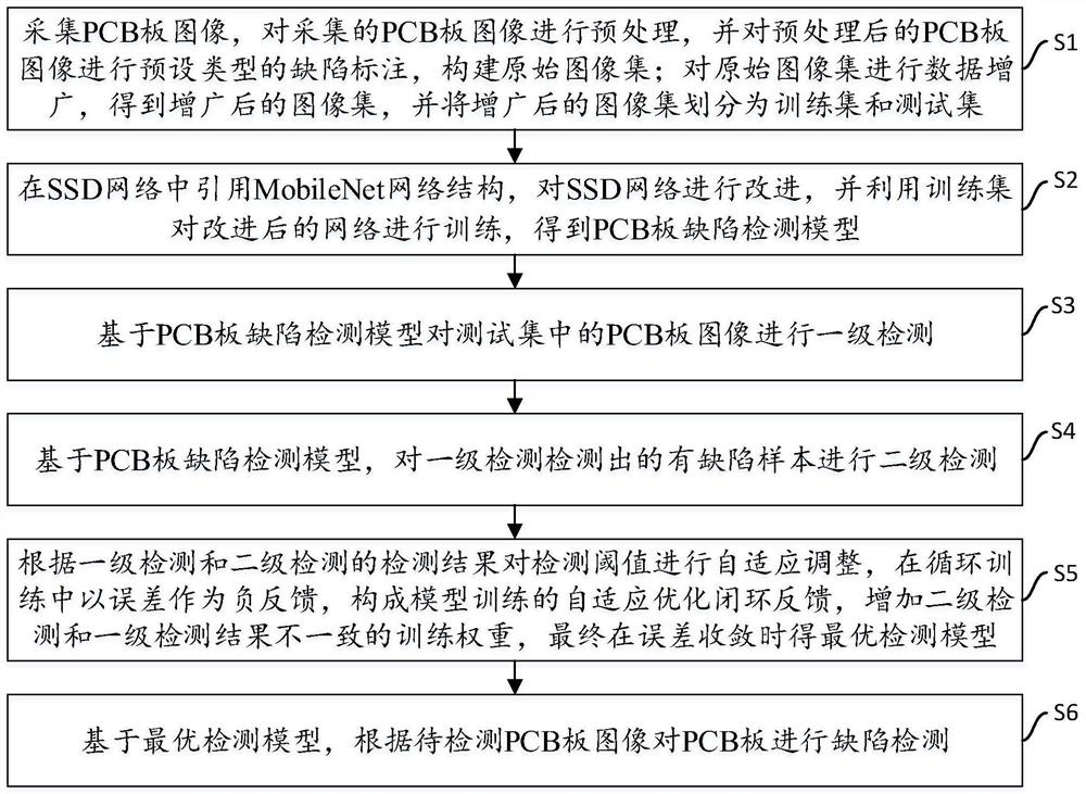
[0049] This embodiment provides a PCB board defect detection method based on re-verification detection, which can be implemented by electronic equipment, and the execution flow of the method is as follows figure 1 shown, including the following steps:

[0050] S1, collect PCB board images, preprocess the collected PCB board images, and mark the pre-processed PCB board images with preset types of defects to construct the original image set; perform data augmentation on the original image set to obtain augmented widened image set, and divide the augmented image set into training set and test set;

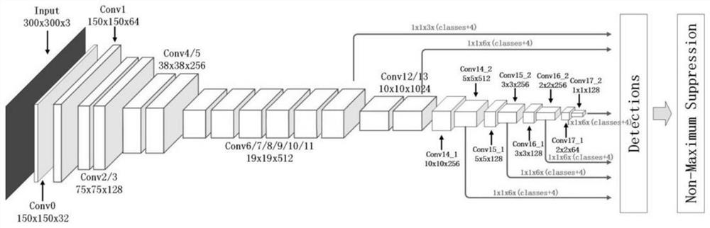
[0051] S2, refer to the MobileNet network structure in the SSD network, improve the SSD network, and use the training set to train the improved network to obtain the PCB board defect detection model;

[0052] S3, based on the PCB board defect detection model, the first-level detection is performed on the PCB board image in the test set;

[0053] S4, based on the PCB board defect det...

no. 2 example

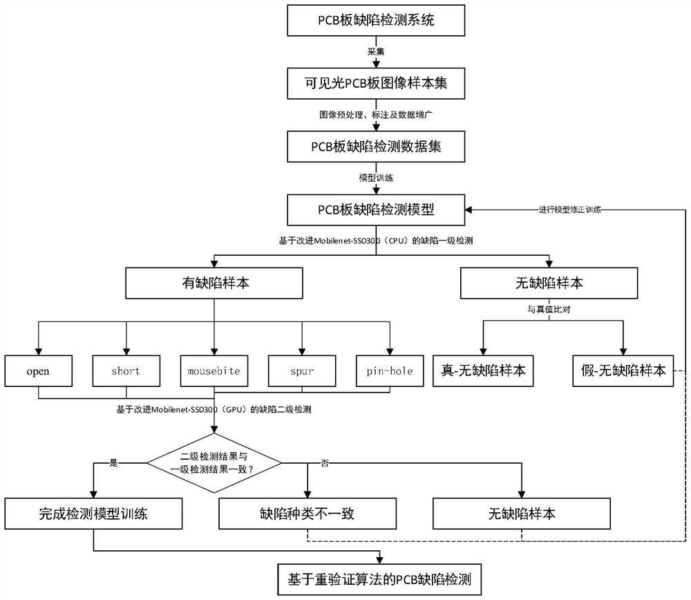
[0058] This embodiment provides a PCB board defect detection method based on re-verification detection, which can be implemented by electronic equipment, and the execution flow of the method is as follows figure 2 shown, including the following steps:

[0059] S1, collect PCB board images, preprocess the collected PCB board images, and mark the pre-processed PCB board images with preset types of defects to construct the original image set; perform data augmentation on the original image set to obtain augmented widened image set, and divide the augmented image set into training set and test set;

[0060] Specifically, in this embodiment, the above S1 includes the following steps:

[0061] S11, use a 1080P visible light camera to collect PCB board images; wherein, when collecting PCB board images, it is required that the chip occupies no less than 60% of the entire image area, and details such as identification numbers and pins are clearly visible;

[0062] S12, using the Can...

no. 3 example

[0082] This embodiment provides an electronic device, which includes a processor and a memory; at least one instruction is stored in the memory, and the instruction is loaded and executed by the processor, so as to implement the method of the foregoing embodiment.

[0083] The electronic device may have relatively large differences due to different configurations or performances, and may include one or more processors (central processing units, CPU) and one or more memories, wherein at least one instruction is stored in the memory, so The above instruction is loaded by the processor and executes the above method.


PUM


Abstract

The invention discloses a PCB defect detection method based on re-verification detection, and the method comprises the steps: collecting a PCB image, and constructing a training set and a test set; introducing MobileNet in the SSD, improving the SSD, and training the improved network by using the training set to obtain a PCB defect detection model; performing primary detection on the PCB image in the test set; performing secondary detection on the defective sample detected by the primary detection; the method comprises the following steps: performing adaptive adjustment on a detection threshold according to detection results of primary detection and secondary detection, forming adaptive optimization closed-loop feedback of model training by taking an error as negative feedback in loop training, increasing a training weight of inconsistent secondary detection and primary detection results, and finally obtaining an optimal detection model during error convergence. Defect detection is realized by using the method. According to the invention, defects of the PCB can be accurately detected, and an over-fitting phenomenon is prevented.

Description

technical field [0001] The present invention relates to the technical fields of target detection and defect detection, in particular to a PCB (printed circuit board, printed circuit board) board defect detection method based on re-verification detection. Background technique [0002] PCB (printed circuit board) is a printed circuit board, referred to as a printed board, and is one of the important components of the electronics industry. Almost every kind of electronic equipment, ranging from electronic watches and calculators to computers, communication electronic equipment, and military weapon systems, as long as there are electronic components such as integrated circuits, in order to make the electrical interconnection between various components, printed circuit boards must be used. plate. [0003] The printed circuit board is composed of an insulating base plate, connecting wires and pads for assembling and welding electronic components, and has the dual functions of a c...

Claims


Application Information

Patent Timeline
Patent Type & Authority Applications(China)
IPC IPC(8): G06T7/00G06T7/11G06T5/00G06K9/62G06V10/774
CPCG06T7/0004G06T7/11G06T5/002G06T2207/20132G06T2207/30141G06T2207/20028G06F18/214
Inventor 彭开香汪倩马亮
Owner UNIV OF SCI & TECH BEIJING
Why Eureka
Try Eureka