Semiconductor structure and forming method thereof

A semiconductor and device structure technology, applied in semiconductor devices, semiconductor/solid-state device manufacturing, transistors, etc., can solve the problems of difficult channel and poor control ability of gate to channel, so as to reduce the probability of blocking and realize The effect of electrical isolation

Pending Publication Date: 2022-04-22
SEMICON MFG INT (SHANGHAI) CORP +1
View PDF0 Cites 4 Cited by
  • Summary
  • Abstract
  • Description
  • Claims
  • Application Information

AI Technical Summary

Problems solved by technology

However, as the channel length of the device is shortened, the distance between the source and the drain of the device is also shortened, so the control ability of the gate to the channel becomes worse, and the gate voltage pinches off the channel. The difficulty is also increasing, making the phenomenon of subthreshold leakage (subthreshold leakage), the so-called short-channel effects (short-channel effects, SCE) more prone to occur

Method used


Image

  • Semiconductor structure and forming method thereof
  • Semiconductor structure and forming method thereof
  • Semiconductor structure and forming method thereof

Examples


Embodiment Construction

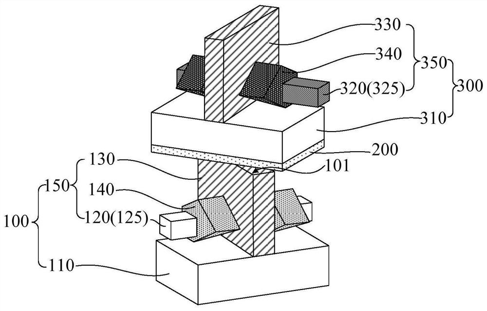
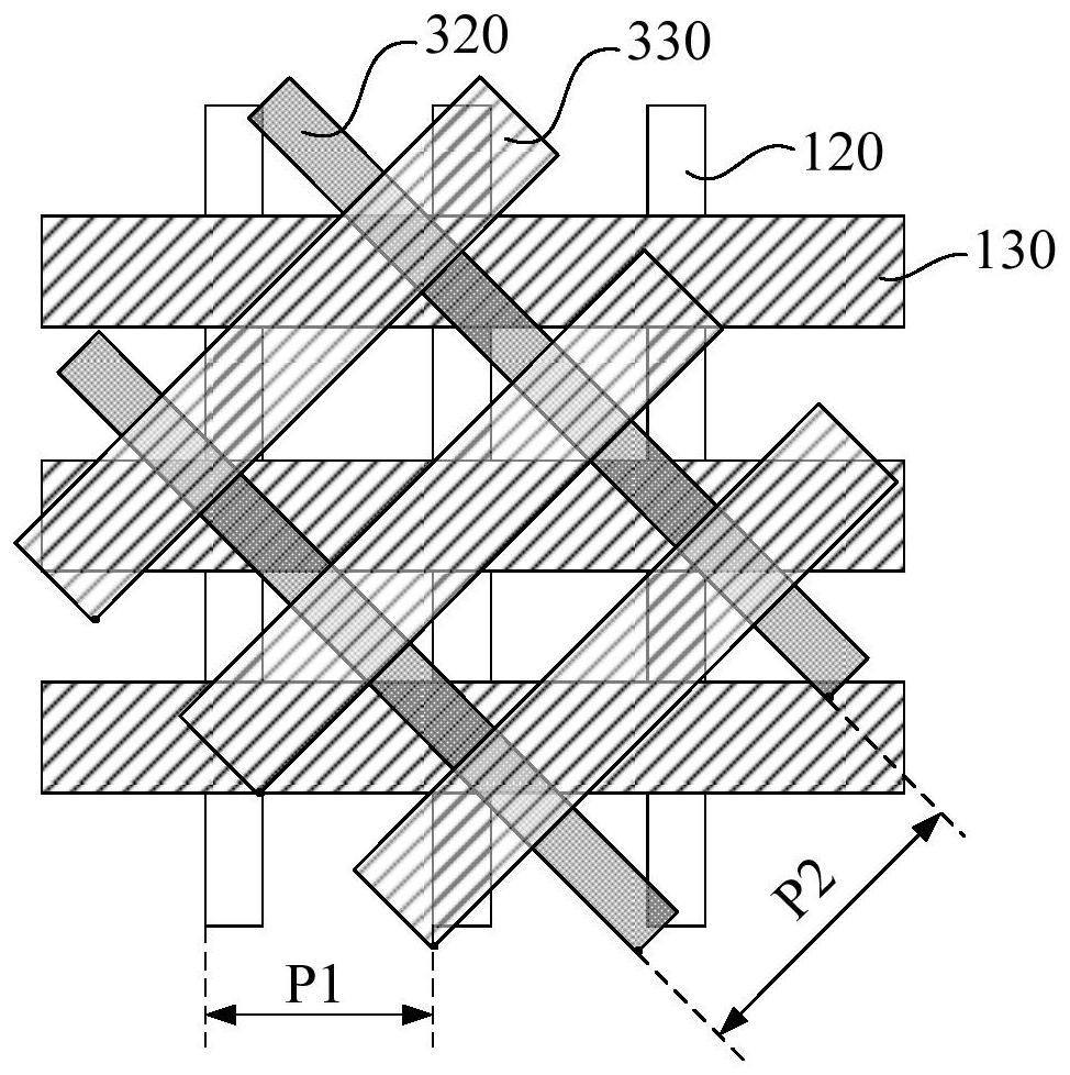
[0016] As known from the background art, the CFET device structure includes a PMOS transistor and an NMOS transistor stacked vertically on each other. However, it is currently difficult to extract the electrical properties of the underlying transistors in the CFET device structure.

[0017] Combining with a semiconductor structure, the reason why it is difficult to extract the electrical properties of the lower layer transistor in the CFET device structure is analyzed.

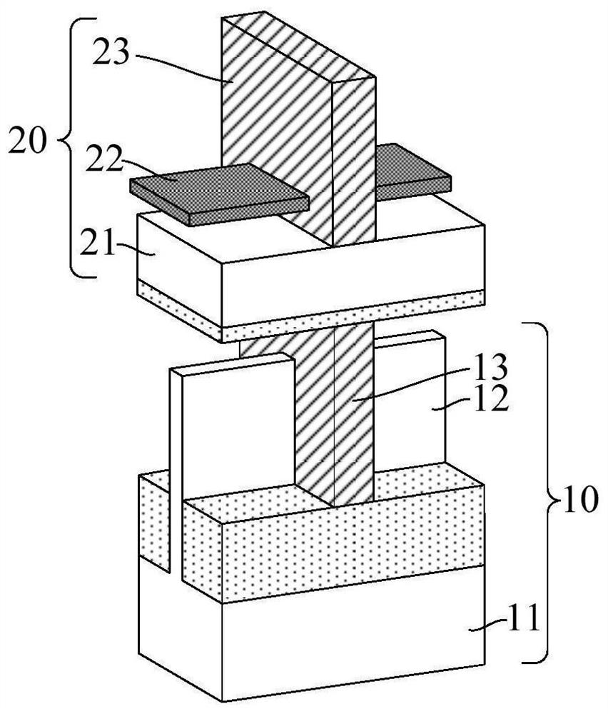
[0018] combined reference figure 1 , showing a perspective view of a semiconductor structure.

[0019] The semiconductor structure includes: a first device structure 10, including a first substrate 11, and a first device (not marked) formed on the first substrate 10, the first device includes a first device located on the first substrate 11 A channel layer structure 12, a first device gate structure 13 across the first device gate structure 12, and a first source and drain in the first channel layer structur...


PUM


Abstract

The invention discloses a semiconductor structure and a forming method thereof, and the semiconductor structure comprises a first device structure which comprises a first substrate and a first device formed on the first substrate, the first device comprises a first channel layer structure located on the first substrate, a first device gate structure crossing the first channel layer structure, and first source-drain doped regions located in the first channel layer structure on the two sides of the first device gate structure; the second device structure is positioned on the front surface of the first device structure and comprises a second substrate positioned on the first device structure and a second device formed on the second substrate; the second device comprises a second channel layer structure located on the second substrate, a second device gate structure crossing the second channel layer structure, and second source-drain doped regions located in the second channel layer structure on the two sides of the second device gate structure; projections of the second channel layer structure and the first channel layer structure on the first substrate are not vertically intersected. According to the invention, electrical leading-out of the first device can be realized.

Description

technical field [0001] Embodiments of the present invention relate to the field of semiconductor manufacturing, and in particular, to a semiconductor structure and a method for forming the same. Background technique [0002] In semiconductor manufacturing, with the development trend of VLSI, the feature size of integrated circuits continues to decrease. In order to accommodate the reduction in feature size, the channel length of MOSFETs has also been shortened accordingly. However, as the channel length of the device is shortened, the distance between the source and the drain of the device is also shortened, so the control ability of the gate to the channel becomes worse, and the gate voltage pinches off the channel. Difficulty is also increasing, making the phenomenon of subthreshold leakage (subthreshold leakage), the so-called short-channel effects (short-channel effects, SCE) more likely to occur. [0003] Therefore, in order to better adapt to the reduction of feature...

Claims


Application Information

Patent Timeline
Patent Type & Authority Applications(China)
IPC IPC(8): H01L27/092H01L21/8238
CPCH01L27/0922H01L27/0924H01L21/8238H01L21/823821H01L2224/83896H01L29/78696H01L29/42392H01L29/66439H01L21/823431H01L27/0886B82Y10/00H01L29/0673H01L29/775H01L27/088H01L27/092H01L27/0688H01L21/8221H01L21/823807H01L21/823871H01L21/823412H01L21/823475H01L25/074H01L25/18H01L25/0657H01L25/50H01L24/29H01L2224/29186H01L29/66742H01L2224/32145H01L2924/13067H01L2924/13069H01L2225/06562H01L29/66795H01L24/32
Inventor 金吉松
Owner SEMICON MFG INT (SHANGHAI) CORP
Why Eureka
Try Eureka