Circuit board pin defect identification method based on feature self-learning
A defect identification and circuit board technology, applied in image data processing, instrumentation, computing, etc., can solve problems such as low severity and frequency, and achieve the effect of reducing workload, reducing missed detection rate, and improving efficiency and accuracy.
- Summary
- Abstract
- Description
- Claims
- Application Information
AI Technical Summary
Problems solved by technology
Method used
Image

Examples
Embodiment Construction
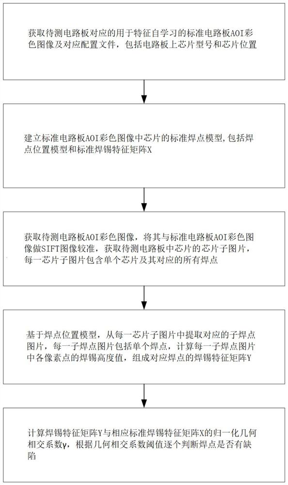
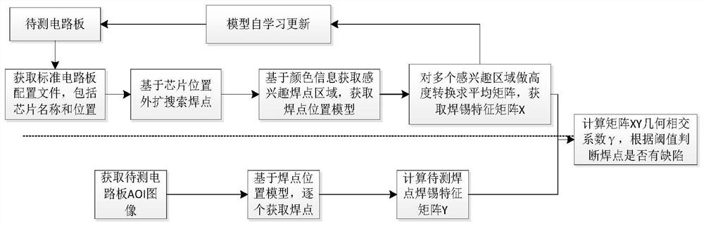
[0041] The application will be further described below in conjunction with the accompanying drawings. The following examples are only used to illustrate the technical solutions of the present invention more clearly, but not to limit the protection scope of the present application.
[0042] like figure 1 and 2 As shown, the circuit board pin defect recognition method based on feature self-learning of the present invention comprises the following steps:
[0043] Step 1: Obtain the AOI color image of the standard circuit board for feature self-learning corresponding to the circuit board to be tested and the corresponding configuration file, including the chip model and chip position on the circuit board;
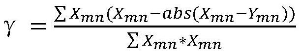
[0044] Step 2: Establish the standard solder joint model of the chip in the AOI color image of the standard circuit board, including the solder joint position model and the standard solder feature matrix X, specifically including:
[0045] Step 2.1: Take the center of the ch...
PUM
 Abstract
Description
Claims
Application Information
 - R&D Engineer
- R&D Manager
- IP Professional
- Industry Leading Data Capabilities
- Powerful AI technology
- Patent DNA Extraction
Browse by: Latest US Patents, China's latest patents, Technical Efficacy Thesaurus, Application Domain, Technology Topic.
© 2024 PatSnap. All rights reserved.Legal|Privacy policy|Modern Slavery Act Transparency Statement|Sitemap