
OLED display panel

A display panel and display area technology, which is applied in the field of OLED display panels, can solve the problems of large internal stress and poor bonding in the support structure of the display module, and achieves the advantages of ensuring normal display, reducing bonding stress and improving bonding yield. Effect

Pending Publication Date: 2022-05-17
WUHAN CHINA STAR OPTOELECTRONICS SEMICON DISPLAY TECH CO LTD
View PDF0 Cites 1 Cited by
  • Summary
  • Abstract
  • Description
  • Claims
  • Application Information

AI Technical Summary

Problems solved by technology

[0005] The present application provides an OLED display panel based on the existing technical problems, which can solve the problem of the small bending radius design of the bending area in the OLED display panel of the prior art, and the support structure of the inner cavity of the bent display module. Large internal stress is generated, which is prone to poor fit

Method used


Image

  • OLED display panel
  • OLED display panel
  • OLED display panel

Examples


Embodiment Construction

[0026] The following descriptions of the various embodiments refer to the accompanying drawings to illustrate specific embodiments in which the invention may be practiced. The directional terms mentioned in the present invention, such as [top], [bottom], [front], [back], [left], [right], [inside], [outside], [side], etc., are only for reference The orientation of the attached schema. Therefore, the directional terms used are used to illustrate and understand the present invention, but not to limit the present invention. In the figure, units with similar structures are indicated by the same reference numerals, and the dotted lines in the figure indicate that they do not exist in the structure, and only illustrate the shape and position of the structure.

[0027] According to the present invention, the bending radius of the bending area in the OLED display panel of the prior art is designed to be small, and the support structure of the inner cavity of the bent display module pr...


PUM


Abstract

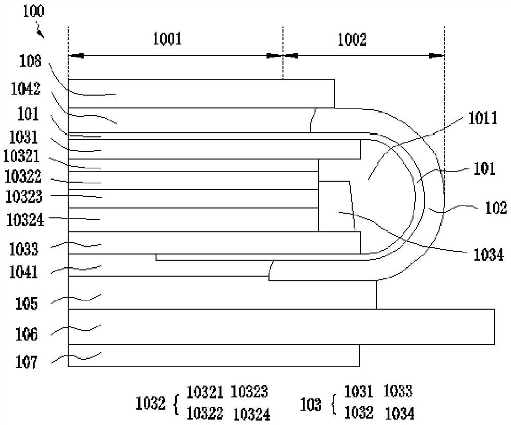
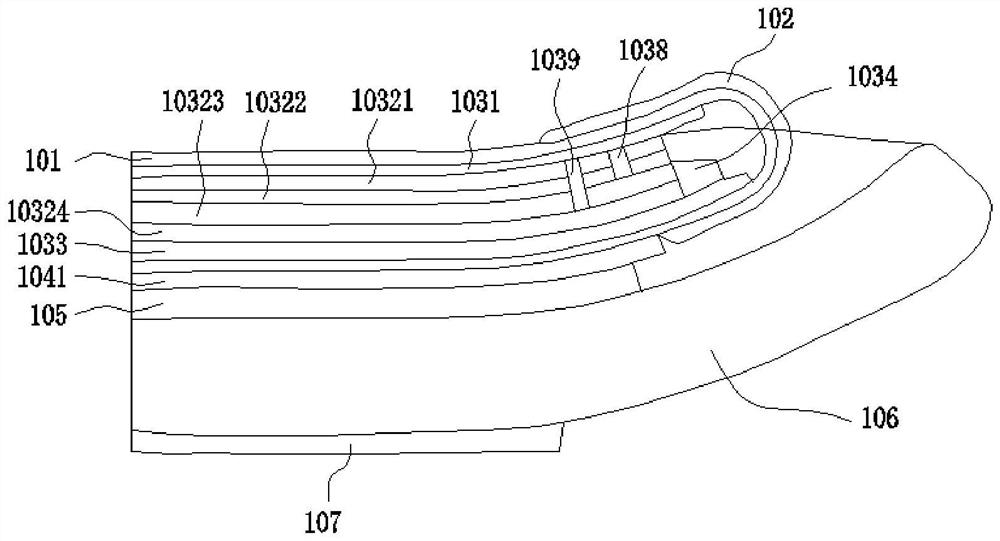
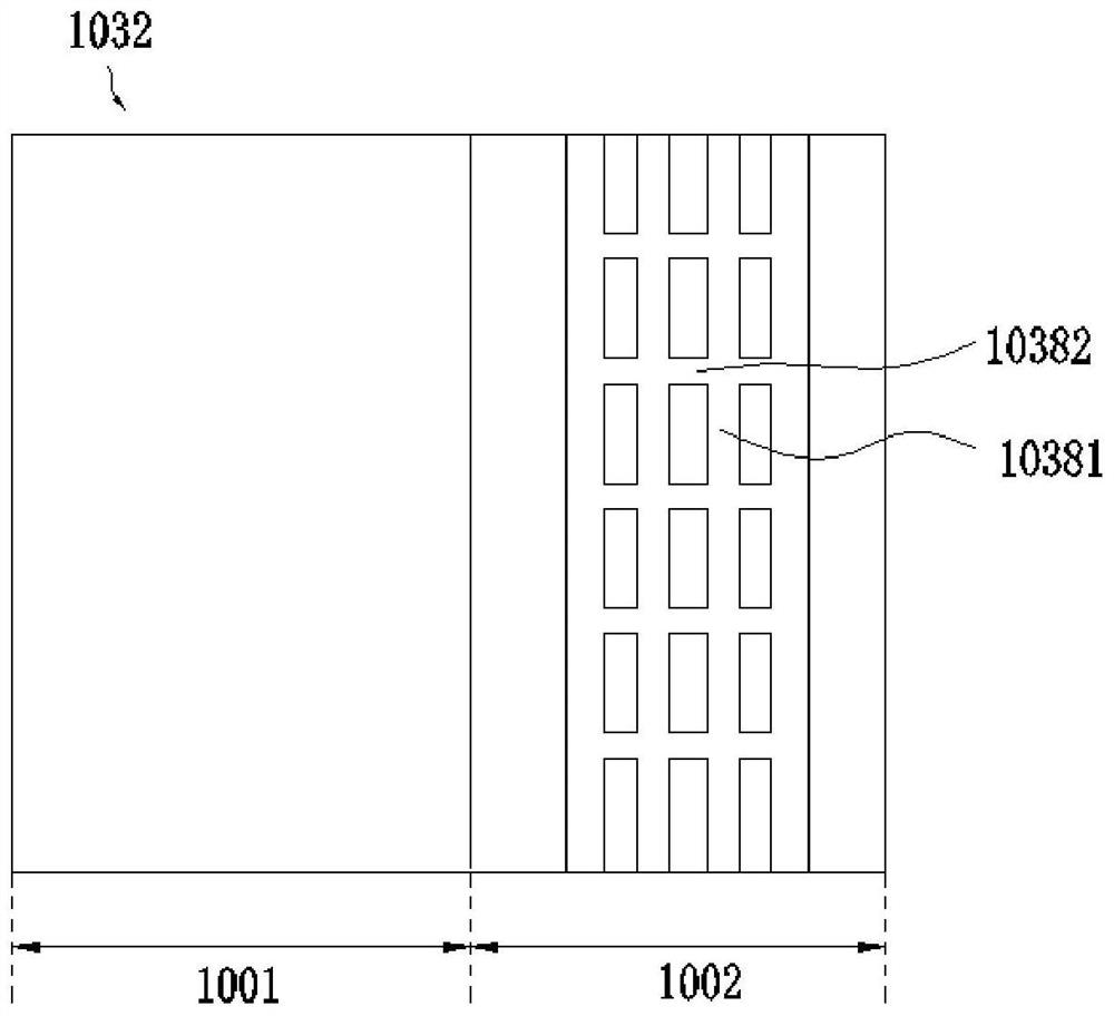
The invention provides an OLED display panel. The OLED display panel comprises a display module, a supporting component located on the back of the display module, and a protective cover plate located on the side, away from the display module, of the supporting component. Wherein the back of the display module is bent to form a containing cavity, and the supporting component is located in the containing cavity; the supporting component comprises a first supporting film, a second supporting film, a stress buffering layer located between the first supporting film and the second supporting film and a supporting block located on the side, close to the bent side of the display module, of the stress buffering layer, wherein the stress buffer layer comprises a grid adhesive layer, a foam layer, a flexible layer and a hardened film which are integrally laminated, and the stress buffer layer is provided with a hollow structure in a non-display area; according to the OLED display panel, an original foam structure and reinforcing plate combined structure is designed into the integrated stress buffer layer, the phenomenon of layer cracking of the OLED display panel in the binding and extruding process is avoided, the lamination stress is reduced through the hollowed-out structure, the lamination yield is improved, and normal display of the display module is guaranteed.

Description

technical field [0001] The present invention relates to the field of display technology, in particular to an OLED display panel. Background technique [0002] OLED display panels have many advantages such as self-illumination, low driving voltage, high luminous efficiency, short response time, high definition and contrast, nearly 180° viewing angle, wide operating temperature range, flexible display and large-area full-color display. It has a wide range of applications in the fields of display, lighting and smart wear. [0003] In order to realize the narrow frame solution of the OLED display panel, it mainly depends on the bending of the bonding area so that the driving chip is bent to the back of the display module. The back of the display panel in the existing display module is generally attached with a SCF (Super Clean Foam, ultra-clean foam) structure and a reinforcing plate. The SCF structure acts as a buffer, and the reinforcing plate acts as a fixation. The height ...

Claims


Application Information

Patent Timeline
IPC IPC(8): H01L27/32G09F9/30
CPCG09F9/301H10K59/10Y02E10/549
Inventor 张冬冬滕飞其他发明人请求不公开姓名
Owner WUHAN CHINA STAR OPTOELECTRONICS SEMICON DISPLAY TECH CO LTD
Learn More