Semiconductor packaging structure and manufacturing method thereof
一种封装结构、半导体的技术,应用在半导体/固态器件制造、半导体器件、半导体/固态器件零部件等方向,能够解决应力敏感、难以实施半导体芯片等问题
- Summary
- Abstract
- Description
- Claims
- Application Information
AI Technical Summary
Problems solved by technology
Method used
Image

Examples
Embodiment Construction
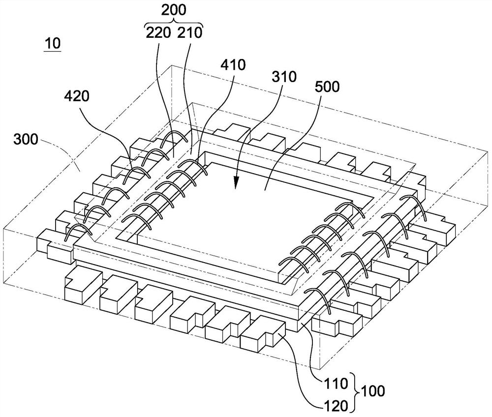
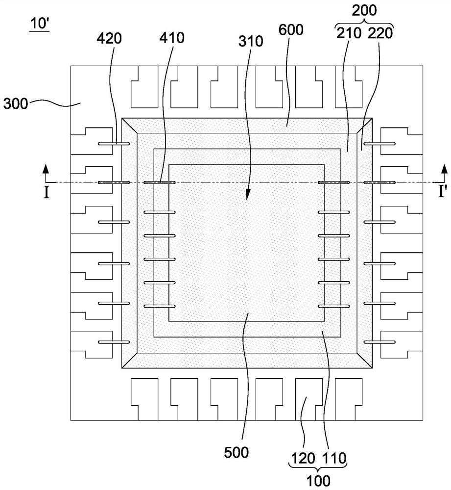
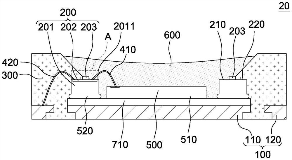
[0019] figure 1 A perspective view illustrating a semiconductor package structure 10 in accordance with some embodiments of the present disclosure. The semiconductor package structure 10 includes a carrier 100 , an interposer 200 , an encapsulant 300 , conductive elements 410 and 420 , and a semiconductor device 500 .
[0020] The carrier 100 may include a substrate, such as an organic substrate or a lead frame. In some embodiments, carrier 100 includes portion 110 and portion 120 spaced from portion 110 from a cross sectional perspective. In some embodiments, portion 110 of carrier 100 includes a paddle or die paddle, and portion 120 of carrier 100 includes one or more leads. In some embodiments, carrier 100 includes one portion 110 (also referred to as "die pad") and a plurality of portions 120 (also referred to as "leads") spaced apart from portion 110 . In some embodiments, portion 110 is surrounded by portion 120 .
[0021] The envelope 300 is on the carrier 100 and d...
PUM
| Property | Measurement | Unit |
|---|---|---|
| density | aaaaa | aaaaa |
| density | aaaaa | aaaaa |
| electrical conductivity | aaaaa | aaaaa |
Abstract
Description
Claims
Application Information