
PCB stacking method based on weight measurement

A PCB board and weight measurement technology, applied in the direction of electrical components, electrical components, etc., can solve the problems of circuit board production scrap, error-prone, increased production costs, etc., to achieve the effect of ensuring the correct rate of pass, type and stacking sequence

Pending Publication Date: 2022-06-28
HUIZHOU XINGSHUNHE ELECTRONICS CO LTD
View PDF0 Cites 0 Cited by
  • Summary
  • Abstract
  • Description
  • Claims
  • Application Information

AI Technical Summary

Problems solved by technology

However, in actual production, there are many types of core boards and prepregs, and it is often easy to make mistakes in the process of stacking boards. There are situations where more or less raw material boards are placed, and raw material types are misplaced, resulting in the scrapping of circuit board production and increasing production costs.

Method used


Image

  • PCB stacking method based on weight measurement

Examples


Embodiment

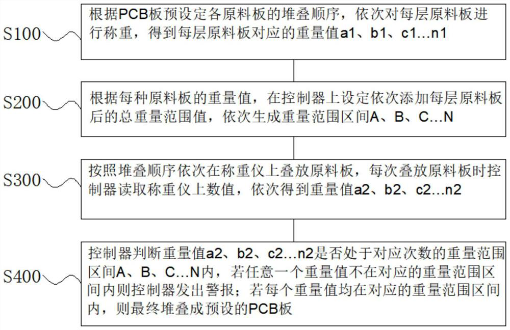
[0016] In order to solve the above technical problems, this embodiment provides a method for stacking PCB boards based on weighing, based on a controller and a precision weighing instrument provided with an alarm, the controller and the precision weighing instrument are connected by signals, and then the controller Can read measurement data on precision weighing scales, such as figure 1 shown, including the following steps:

[0017] S100 , pre-setting the stacking sequence of each raw material board according to the PCB board, and weighing each layer of raw material boards in turn to obtain weight values ​​a1, b1, c1...n1 corresponding to each layer of raw material boards;

[0018] According to the structural requirements of the customer's final PCB board, the stacking sequence of each raw material board is designed, wherein each raw material board may include No. 1 core board, No. 2 core board, No. 3 core board, etc., as well as No. 1 prepreg, No. 2 prepreg Etc., the weight ...


PUM


Abstract

The invention relates to the technical field of circuit board manufacturing, in particular to a PCB stacking method based on weight measurement, which comprises the following steps of: presetting a stacking sequence of each raw material board according to a PCB, sequentially weighing each layer of raw material board to obtain a weight value corresponding to each layer of raw material board, and then according to the weight value of each type of raw material board, carrying out weight measurement on the raw material board according to the weight value of each type of raw material board. Setting a total weight range value after each layer of raw material plates are sequentially added on the controller, sequentially generating weight range intervals, reading numerical values on the weighing instrument by the controller when the raw material plates are stacked each time, sequentially obtaining weight values, judging whether the weight values are in the weight range intervals of the corresponding times by the controller, and if yes, judging whether the weight values are in the weight range intervals of the corresponding times; therefore, whether the models and the number of the raw material boards stacked each time are correct or not can be detected, so that the type and the stacking sequence of each raw material board are correct, the situations of excessive placement, insufficient placement and wrong placement of the raw material types of the raw material boards in the board stacking process are prevented, and the qualified rate of processing and forming of the multi-layer PCB is ensured.

Description

technical field [0001] The invention relates to the technical field of circuit board fabrication, in particular to a method for stacking PCB boards based on weight measurement. Background technique [0002] The circuit board substrate usually includes a core board, a prepreg and other multi-layer raw material board structures, and there are different models of the core board and the prepreg. The weight of each type of core board and prepreg is different. In the combined production process of the circuit board , it is usually necessary to stack multiple raw material boards and complete the pressing process. During the stacking process, the circuit board stacks need to be stacked in the set order to form the required circuit board structure. Therefore, in the stacking process of the raw material boards There can be no sequence errors in the process. However, in actual production, there are many types of core boards and prepregs, and mistakes are often made in the process of s...

Claims


Application Information

Patent Timeline
Patent Type & Authority Applications(China)
IPC IPC(8): H05K13/08
CPCH05K13/085
Inventor 包光先姜辉曹新臣吴述金张裕伟
Owner HUIZHOU XINGSHUNHE ELECTRONICS CO LTD
Learn More