Reflective modulator and image display device
A light modulator, reflective technology, used in instruments, image communications, static indicators, etc., to solve problems such as poor efficiency
- Summary
- Abstract
- Description
- Claims
- Application Information
AI Technical Summary
Problems solved by technology
Method used
Image

Examples
no. 1 example
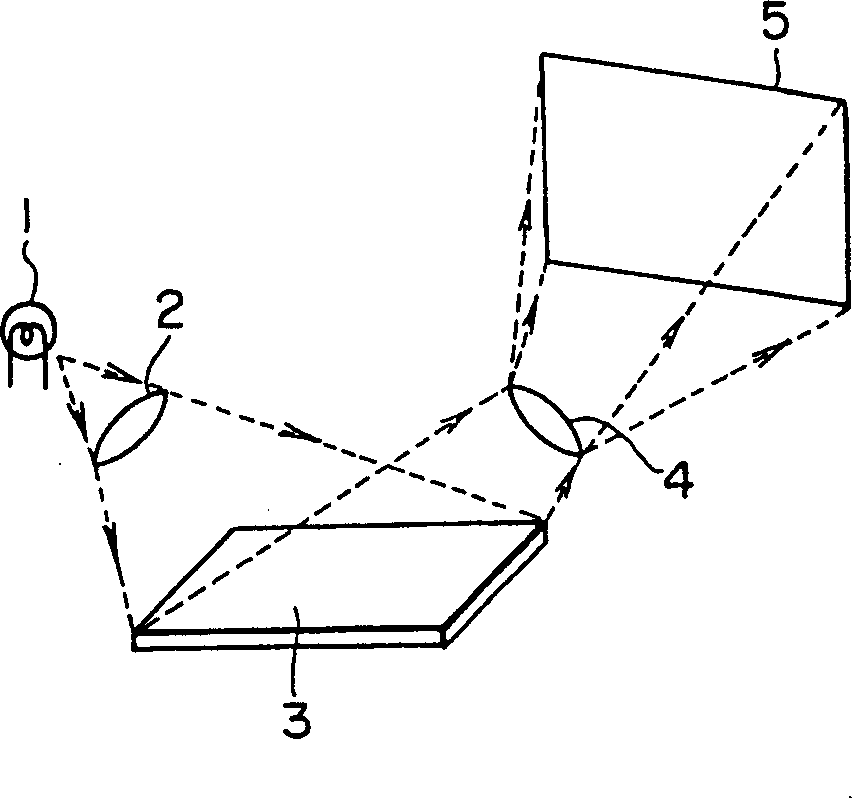
[0098] First, the first embodiment will be described in which the modulation layer 8 does not have a memory characteristic state, and therefore, it is necessary to maintain the electric field applied to the modulation layer 8 while an image is being displayed. In other words, since the modulation layer 8 does not have the memory characteristic state as described above, an electric field must be continuously applied to the modulation layer 8 in order to maintain the driving state of the modulation layer 8 . It should be noted that, on the other hand, in the case where the modulation layer 8 has a memory characteristic state, once the modulation layer 8 is in the driven state, it is no longer necessary to continuously maintain the electric field applied to the modulation layer 8 .
[0099] In this example, if Figure 5 and 6 As shown, a control line 25 is generated on the driving layer 6 of the optical spatial modulator 3, and each storage unit 12 of the optical spatial modulat...
no. 2 example
[0117] A second embodiment in which it is necessary to neutralize residual charges in the modulation layer 8 is described below. It should be noted that, in the second embodiment, a light modulation material capable of changing the light modulation state in response to an applied electric field regardless of the polarity of the electric field is used as the material of the modulation layer 8 . That is, in the case of the second embodiment, the modulation layer 8 is in a driven state when a positive electric field or a negative electric field generated by the driving layer 6 is applied to the modulation layer 8 . On the other hand, modulation layer 8 is in an initial state when no electric field is applied thereto.
[0118] In the second embodiment, as Figure 9 and 10 As shown, a first control line 36 and a second control line 37 are generated on the driving layer 6 of the optical spatial modulator 3, and each storage unit 12 of the optical spatial modulator 3 is designed to...
no. 3 example
[0132] In the case of the third embodiment, a light modulation material having memory characteristics (for example, FLC and PDLC) is used as the material of modulation layer 8 . When displaying an image, an electric field is applied to the modulation layer 8 only when it is necessary to change the modulation layer 8 from the initial state to the driving state. The modulation layer 8 is reset to the initial state before displaying the next image.
[0133] In the third embodiment, such as Figure 13 and 14 As shown, the first control line 46, the second control line 47 and the third control line 48 are produced on the driving layer 6 of the optical spatial modulator 3, and each storage unit 12 of the optical spatial modulator 3 is designed to include the first A memory 41, a second gate circuit 42, a second memory 43, a second gate circuit 4 and a driver 45, such as Figure 15 shown. The second memory 43 used in the storage unit 12 is used to store pixel data of an image bei...
PUM
 Abstract
Description
Claims
Application Information
 - R&D
- Intellectual Property
- Life Sciences
- Materials
- Tech Scout
- Unparalleled Data Quality
- Higher Quality Content
- 60% Fewer Hallucinations
Browse by: Latest US Patents, China's latest patents, Technical Efficacy Thesaurus, Application Domain, Technology Topic, Popular Technical Reports.
© 2025 PatSnap. All rights reserved.Legal|Privacy policy|Modern Slavery Act Transparency Statement|Sitemap|About US| Contact US: help@patsnap.com