
Chip input and output module arrangement method and device and storage medium

A technology of input and output modules and chips, which is applied in the directions of instruments, calculations, and electrical digital data processing, etc., can solve the problems of increased difficulty in chip IO layout, reduced chip IO space, and high design costs, so as to meet the rationality of outgoing lines and signal Integrity requirements, the effect of improving layout efficiency

Pending Publication Date: 2022-07-01
GUANGDONG OPPO MOBILE TELECOMM CORP LTD
View PDF0 Cites 0 Cited by
  • Summary
  • Abstract
  • Description
  • Claims
  • Application Information

AI Technical Summary

Problems solved by technology

Since the chip IO is usually placed on the edge of the chip, when the chip manufacturing process develops below 10nm, the space for chip IO arrangement will be further reduced, which brings challenges to the chip IO arrangement, and the difficulty of chip IO arrangement will further increase. Large, the layout plan needs to be adjusted repeatedly, the workload is heavy, and human errors are prone to occur, the design cost is high, and the design cycle is long

Method used


Image

  • Chip input and output module arrangement method and device and storage medium
  • Chip input and output module arrangement method and device and storage medium
  • Chip input and output module arrangement method and device and storage medium

Examples


Embodiment Construction

[0018] The present disclosure describes various embodiments, but the description is exemplary rather than restrictive, and it will be apparent to those of ordinary skill in the art that within the scope of the embodiments described in this disclosure can be There are many more examples and implementations.

[0019] In the description of the present disclosure, the words "exemplary" or "such as" are used to mean serving as an example, illustration, or illustration. Any embodiment described in this disclosure as "exemplary" or "such as" should not be construed as preferred or advantageous over other embodiments. In this article, "and / or" is a description of the association relationship between associated objects, indicating that there can be three kinds of relationships, for example, A and / or B, which can mean that A exists alone, A and B exist simultaneously, and exist independently B these three cases. "Plurality" means at least two, including two or more than two. In addit...


PUM


Abstract

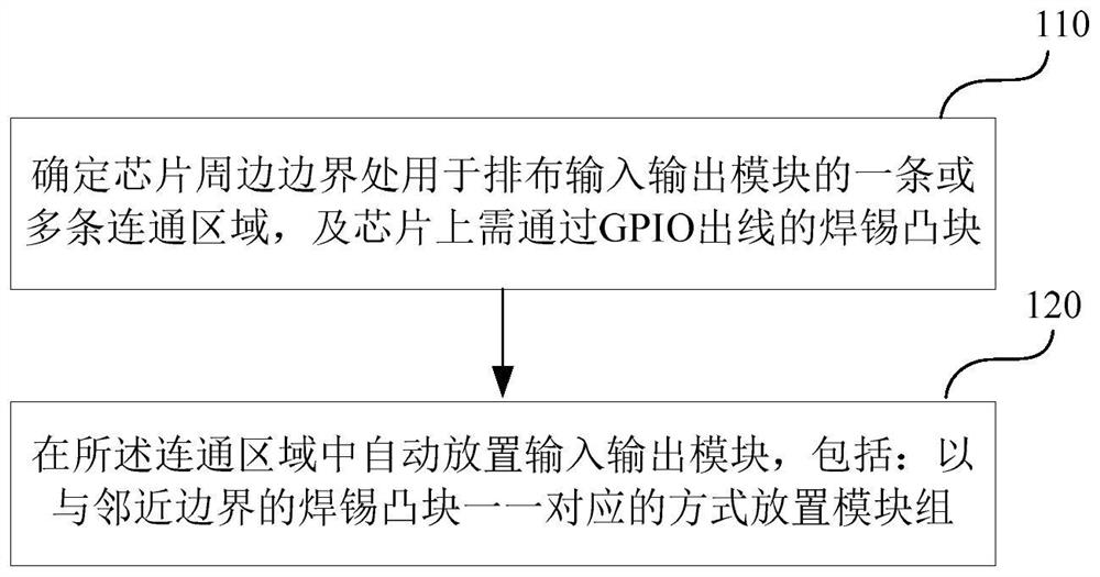
The invention discloses a chip input and output module arrangement method and device and a storage medium. The method comprises the following steps: firstly, determining one or more communication regions for arranging input and output modules at the peripheral boundary of a chip, and a soldering tin bump needing to pass through a GPIO (General Purpose Input / Output) outgoing line on the chip; and automatically placing an input / output module in the communication area, wherein module groups are placed in a one-to-one correspondence manner with the soldering tin bumps adjacent to the boundary. The embodiment of the invention further provides a device for implementing the method. According to the embodiment of the invention, automatic arrangement of the input and output modules of the chip can be adaptively realized, so that the input and output modules of the chip meet the requirements of wire outgoing rationality and signal integrity, and the arrangement efficiency is greatly improved.

Description

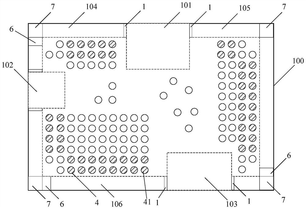
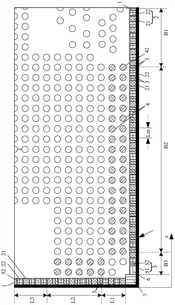
technical field [0001] The present disclosure relates to, but is not limited to, chip technology, and more particularly, to a method, device, and storage medium for arranging chip input and output modules. Background technique [0002] With the development of Moore's Law, the chip scale is further reduced, which puts forward higher requirements for chip design. The chip input and output module (IO: Input and Output) is an important part of the chip design. It is mainly used to input the external signals required for the chip to work and output the processed signals to the outside world. There are also some other modules for assist in this work. Common chip IOs include general purpose input / output modules (GPIO: General Purpose Input / Output), power supply modules, power control modules, termination modules, corner modules, common filling modules, and the like. Since the chip IO is usually placed on the edge of the chip, when the chip process develops below 10nm, the space f...

Claims


Application Information

Patent Timeline
Patent Type & Authority Applications(China)
IPC IPC(8): G06F30/392G06F30/398
CPCG06F30/392G06F30/398
Inventor 李可
Owner GUANGDONG OPPO MOBILE TELECOMM CORP LTD
Learn More