Sampling compensation method and device of digital channel logic analyzer

A logic analyzer and digital channel technology, applied in measuring devices, instruments, measuring electronics, etc., can solve the problems of high price, high cost of delay chips, limited number of high-speed transmission interfaces, etc., achieve high resolution and small hardware changes , the effect of low sampling cost

Pending Publication Date: 2022-07-05
杭州加速科技有限公司
View PDF12 Cites 0 Cited by
  • Summary
  • Abstract
  • Description
  • Claims
  • Application Information

AI Technical Summary

Problems solved by technology

[0008] The high-speed interface sampling method is to connect the digital signal to the high-speed transmission interface (GTP) of the FPGA for sampling, and the sampling rate can reach tens of GHZ. However, the high-speed transmission interface of the FPGA is limited and expensive, and cannot meet the channel number requirements of the test equipment.
[0009] The external multi-channel delay sampling method is often used in the design of high-speed analog oscilloscopes. In this method, the signal is fanned out into multiple signals, and each signal is delayed according to the law, and the multiple delayed signals are sampled and processed. The sampling signal is obtained by interpolation. This method is not only because of the high cost of the external delay chip, but also the delayed signal requires a large number of pins to be input to the FPGA for sampling, and the digital pins of the semiconductor test equipment are connected to the FPGA after passing through the PE chip in a fixed form. Therefore, this method cannot be directly introduced into the digital channel logic analyzer of semiconductor test equipment

Method used


Image

  • Sampling compensation method and device of digital channel logic analyzer
  • Sampling compensation method and device of digital channel logic analyzer
  • Sampling compensation method and device of digital channel logic analyzer

Examples


Embodiment 1

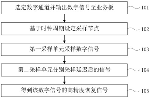
[0060] Embodiment 1 of the present invention discloses a sampling compensation method for a digital channel logic analyzer in an ATE device, which can realize high-resolution sampling. The flow chart of the sampling compensation method is attached to the instruction manual figure 1 As shown, the specific scheme is as follows:

[0061] A sampling compensation method for a digital channel logic analyzer in ATE equipment, comprising the following steps:

[0062] 101. Select the digital channel of the chip, and output the digital signal to the service board through the digital channel;

[0063] 102. Set a sampling node based on the clock cycle of the preset clock signal, and control the first sampling unit and the second sampling unit to perform sampling when each clock cycle passes through the sampling node;

[0064] 103. Sampling the digital signal by the first sampling unit to obtain first sampling data;

[0065] 104. Delay the digital signal through each sub-chain of the de...

Embodiment 2

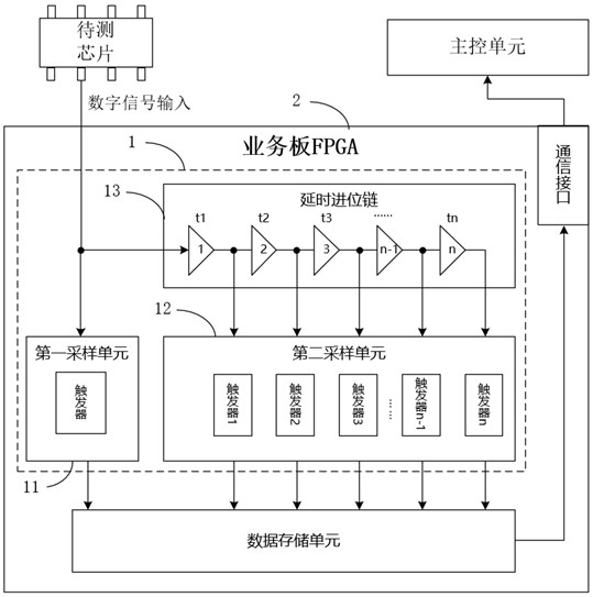
[0094] Embodiment 2 of the present invention discloses a sampling compensation device for a digital channel logic analyzer in ATE equipment, which is used to implement the sampling method of Embodiment 1. The sampling compensation device is shown in Figure 2 of the specification, and the specific scheme is as follows:

[0095] A sampling compensation device for a digital channel logic analyzer in ATE equipment, the sampling compensation device 1 is located on a service board FPGA2, and includes a first sampling unit 11, a second sampling unit 12 and a delay carry chain 13;

[0096] The first sampling unit 11 is configured with a trigger for directly sampling the digital signal received by the service board FPGA to obtain the first sampling data;

[0097] The delay carry chain 13 is composed of a plurality of sub-chains connected in series in sequence, and the output end of each sub-chain is connected to the second sampling unit, and is used for delaying the received digital si...


PUM


Abstract

The invention provides a sampling compensation method and device for a digital channel logic analyzer. The method comprises the following steps: selecting a digital channel of a chip and outputting a digital signal to a service board; setting a sampling node based on a clock period; the first sampling unit samples the digital signal to obtain first sampling data; the delay carry chain delays the digital signal and outputs the delayed digital signal of each sub-chain to the second sampling unit; the second sampling unit samples the delayed digital signal and analyzes the digital signal to obtain compensation data; and according to whether the first sampling data and the second sampling data have level change, combining the compensation data to obtain a high-precision recovery signal of the digital signal. According to the scheme, high-resolution parallel sampling can be achieved, the real phase relation of digital signals can be restored through real sampling, narrow-pulse-width digital signal noise can be captured, limitation of the number of digital channels is avoided, extra hardware cost does not need to be increased, and the sampling cost is low.

Description

technical field [0001] The invention relates to the field of semiconductor chip testing, in particular to a sampling compensation method and device for a digital channel logic analyzer. Background technique [0002] ATE (Automatic Test Equipment) is an integrated circuit automatic test equipment, which is a special equipment used to detect the function and performance of chips. The DIO digital channel is the core functional module of the integrated circuit test equipment, which is responsible for the work of generating digital waveforms in chip testing and outputting them to the chip and receiving the digital signals output by the chip and comparing and judging. [0003] In the actual chip test, due to the various uncertainties in the actual output signal of the chip to be tested, when the automated test equipment fails to compare the signal received by the digital channel with the expected signal, it is necessary to perform physical analysis on the digital signal output by ...

Claims


Application Information

Patent Timeline
IPC IPC(8): G01R31/3177
CPCG01R31/3177
Inventor 陈永邬刚
Owner 杭州加速科技有限公司
Why Eureka
Try Eureka