Multi-axis sheet feeding system for semiconductor equipment

A semiconductor and equipment technology, applied in the field of multi-axis wafer feeding system for semiconductor equipment, can solve problems such as the inability to meet high-quality or special semiconductor material preparation conditions, meet special process movement requirements, improve compactness, and realize temperature dynamic testing Effect

Pending Publication Date: 2022-07-05
48TH RES INST OF CHINA ELECTRONICS TECH GROUP CORP
View PDF0 Cites 0 Cited by
  • Summary
  • Abstract
  • Description
  • Claims
  • Application Information

AI Technical Summary

Problems solved by technology

Obviously, the existing single-substrate boat mechanism with a fixed temperature measurement point can only meet the preparation of ordinary semiconductor materials, but cannot meet the preparation conditions of high-quality or special semiconductor materials.

Method used


Image

  • Multi-axis sheet feeding system for semiconductor equipment
  • Multi-axis sheet feeding system for semiconductor equipment
  • Multi-axis sheet feeding system for semiconductor equipment

Examples


Embodiment

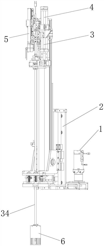
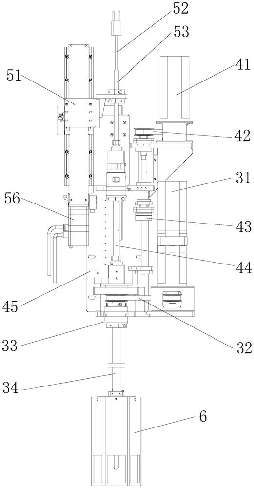
[0033] like Figure 1 to Figure 9As shown, the multi-axis wafer feeding system for semiconductor equipment of the present invention includes: a first driving assembly 1, a first lifting assembly 2, an outer boat assembly 3, an inner boat assembly 4, a thermocouple assembly 5 and a Boat frame assembly 6. The outer boat assembly 3, the inner boat assembly 4, the thermocouple assembly 5 and the boat frame assembly 6 form a multi-axis film feeding unit, and the multi-axis film feeding unit is connected with the first lifting assembly 2, and the output end of the first driving assembly 1 is connected with the first lifting assembly 2. A lift assembly 2 is connected, and the multi-axis wafer feeding unit cooperates with the first drive assembly 1 and the first lift assembly 2 to realize the transfer of the substrate to the semiconductor equipment and complete the corresponding coating process.

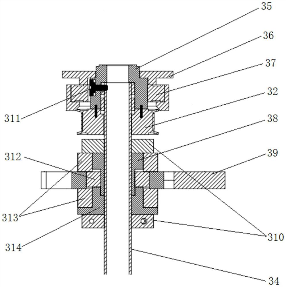
[0034] The outer boat assembly 3 includes a second drive assembly 31 and an outer boat ...


PUM


Abstract

The invention discloses a multi-shaft wafer feeding system for semiconductor equipment, which comprises a first driving assembly, a first lifting assembly and a multi-shaft wafer feeding unit consisting of an outer boat assembly, an inner boat assembly, a thermocouple assembly and a boat frame assembly, and is characterized in that the first driving assembly drives the first lifting assembly to drive the multi-shaft wafer feeding unit to lift in a reciprocating manner; the outer boat assembly comprises a second driving assembly and an outer boat frame connecting rod, the inner boat assembly comprises a third driving assembly and an inner boat frame connecting rod, the thermocouple assembly comprises a thermocouple and a fourth driving assembly, and the thermocouple, the inner boat frame connecting rod and the outer boat frame connecting rod are sequentially installed in a nested mode. The third driving component drives the inner boat frame connecting rod to lift and move the boat frame component loaded with the substrate into or out of the growth mother solution; the second driving assembly drives the outer boat frame connecting rod to rotate and drives the boat frame assembly to rotate, so that substrate coating is completed; and the fourth driving assembly drives the thermocouple to lift so as to test the temperature of different parts of the reaction chamber. The method has the advantages of simple operation, high control precision, flexible and changeable temperature measurement points and the like.

Description

technical field [0001] The invention belongs to the technical field of semiconductors, and in particular relates to a multi-axis sheet feeding system for semiconductor equipment. Background technique [0002] With the rapid development of the semiconductor industry and the blockade of our technology by European and American countries, it is more urgent for the country to develop semiconductor equipment technology. The core of the semiconductor equipment motion system is the dynamic measurement of substrate transportation and reaction chamber process temperature. Most of the substrate transportation of existing semiconductor equipment is a simple uniaxial mechanism, that is, the substrate is directly transferred to the process chamber in a straight line, and the temperature measurement point on the substrate is fixed, so it is impossible to detect real-time detection of different positions within the constant temperature zone of the reaction chamber. process temperature. Th...

Claims


Application Information

Patent Timeline
Patent Type & Authority Applications(China)
IPC IPC(8): H01L21/677H01L21/67
CPCH01L21/67742H01L21/67248
Inventor 陈李松李军黄志海马国威张超
Owner 48TH RES INST OF CHINA ELECTRONICS TECH GROUP CORP
Why Eureka
Try Eureka