Series assembly equipment and method for solar cell silicon wafers

A technology of solar cells and battery silicon wafers, applied in circuits, electrical components, photovoltaic power generation, etc., can solve the problems of limited welding space, inconvenient serial assembly of silicon wafers, etc., and achieve the effect of achieving tightness and increasing contact area.

Active Publication Date: 2022-07-08
晟高发新能源发展(江苏)有限公司
View PDF6 Cites 0 Cited by
  • Summary
  • Abstract
  • Description
  • Claims
  • Application Information

AI Technical Summary

Problems solved by technology

[0004] The purpose of the present invention is to provide a series assembly equipment for solar cell silicon wafers, another purpose is to provide an assembly method for solar battery silicon wafers series assembly equipment, through the setting of the plug board and the plug interface, to solve the above background The silicon chip welding space proposed in the technology has certain limitations, which makes it inconvenient for the serial assembly of silicon chips

Method used


Image

  • Series assembly equipment and method for solar cell silicon wafers
  • Series assembly equipment and method for solar cell silicon wafers
  • Series assembly equipment and method for solar cell silicon wafers

Examples


Embodiment Construction

[0033] The present invention will be described in further detail below with reference to the accompanying drawings and specific embodiments. The embodiments of the present invention are presented for purposes of illustration and description, and are not intended to be exhaustive or to limit the invention to the forms disclosed. Many modifications and variations will be apparent to those of ordinary skill in the art. The embodiment was chosen and described in order to better explain the principles of the invention and the practical application, and to enable others of ordinary skill in the art to understand the invention for various embodiments with various modifications as are suited to the particular use.

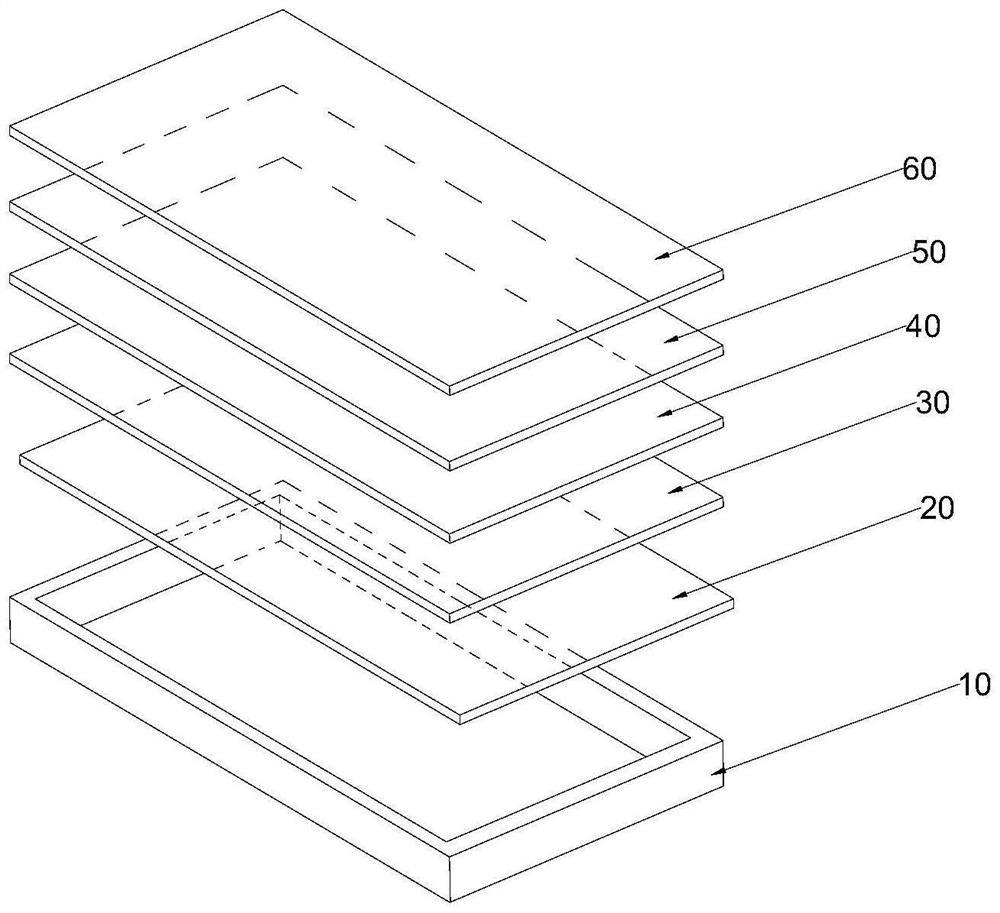
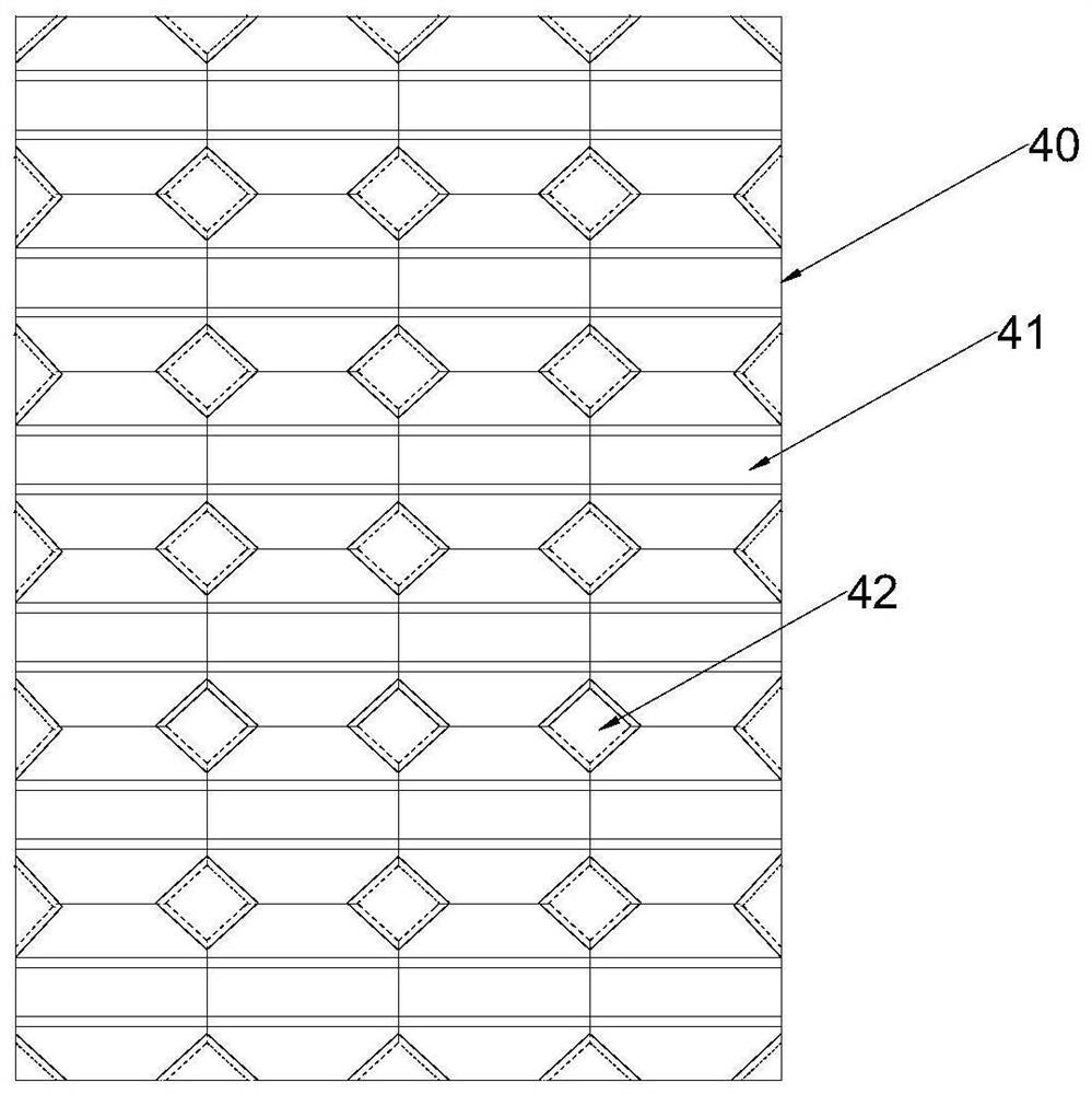
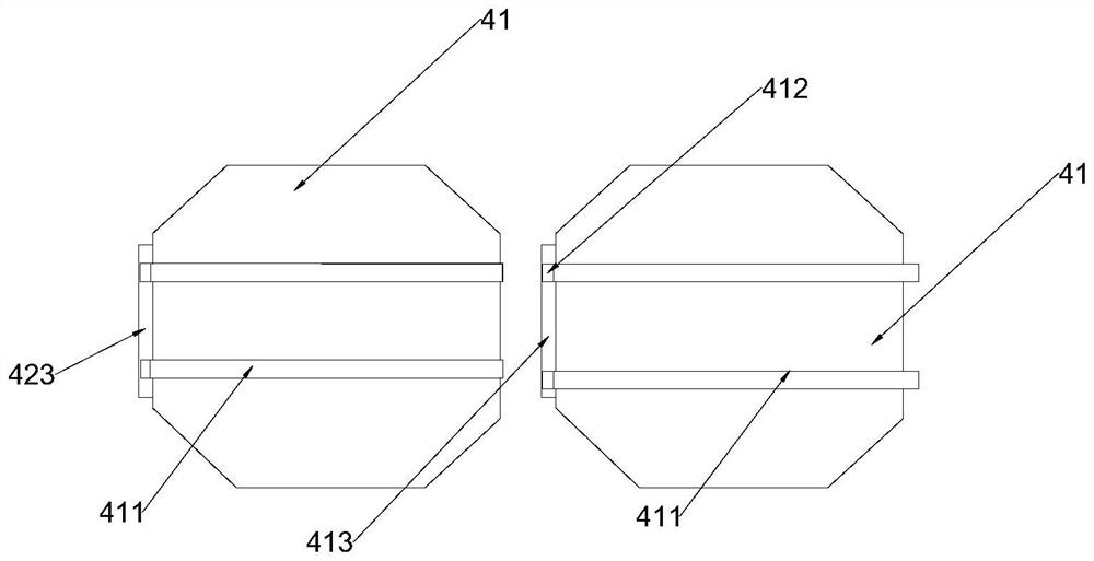
[0034] see Figure 1-Figure 8 , In the embodiment of the present invention, a solar cell silicon wafer serial assembly device and method, wherein the assembly device includes an aluminum alloy frame 10, a back plate 20, a first EVA board 30, a battery silicon wafer board ...


PUM


Abstract

The invention discloses a series assembly device and method for solar cell silicon wafers, and belongs to the technical field of assembly equipment, the series assembly device comprises a cell silicon wafer plate body, the cell silicon wafer plate body is made of a plurality of silicon wafers and a plurality of assembly parts, the plurality of silicon wafers are assembled together through the assembly parts, the silicon wafers are provided with a plurality of first conductive sheets, and the first conductive sheets are arranged on the silicon wafers. One end of the first conducting strip is fixedly connected with a second conducting strip, the other end of the first conducting strip is fixedly connected with a third conducting strip, one end, close to the second conducting strip, of the silicon wafer is fixedly connected with a plug board, and one end, close to the third conducting strip, of the silicon wafer is provided with a plug port. The tightness between the second conducting strip and the third conducting strip is realized, the contact area between the silicon wafers is increased by using the plugging of the plugging plate and the plugging port, and meanwhile, the second conducting strip and the third conducting strip which are plugged are connected together in an electrocoagulation manner, so that the electrification between the plurality of silicon wafers is realized.

Description

technical field [0001] The invention relates to the field of assembling equipment, in particular to a serial assembling equipment and method of solar cell silicon wafers. Background technique [0002] Silicon wafers are often used in the production of solar photovoltaic panels. The content of silicon in the earth's crust is 25.8%, which provides an inexhaustible source for the production of monocrystalline silicon. The advantage of reserves is also one of the reasons why silicon has become the main photovoltaic material. When multiple silicon wafers are connected in series to prepare solar silicon wafers, when the silicon wafers are assembled in series, the copper wafers arranged on the silicon wafers realize the series connection between the silicon wafers. [0003] When silicon wafers are used in the production of solar cell photovoltaic panels, due to the loss of lifting force at the series connection of the silicon wafers, the connection of the silicon wafers is prone to...

Claims


Application Information

Patent Timeline
Patent Type & Authority Applications(China)
IPC IPC(8): H01L31/18H01L31/05
CPCH01L31/1876H01L31/0504Y02P70/50
Inventor 邵建海孔德明
Owner 晟高发新能源发展(江苏)有限公司
Why Eureka
Try Eureka