

Semiconductor device and manufacturing method thereof
A semiconductor and device technology, applied in the field of semiconductor devices, can solve the problems that the bonding wire cannot be wrapped in the package PC, exposed, and the bending height is high
- Summary
- Abstract
- Description
- Claims
- Application Information
AI Technical Summary
Problems solved by technology
Method used
Image

Examples
Embodiment Construction
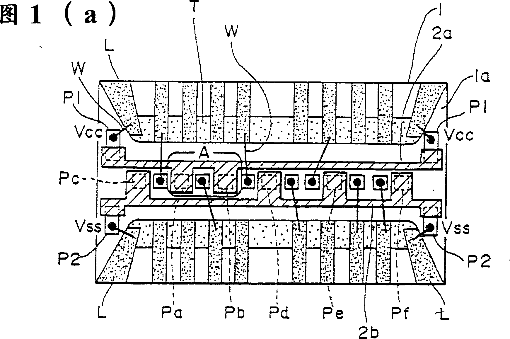
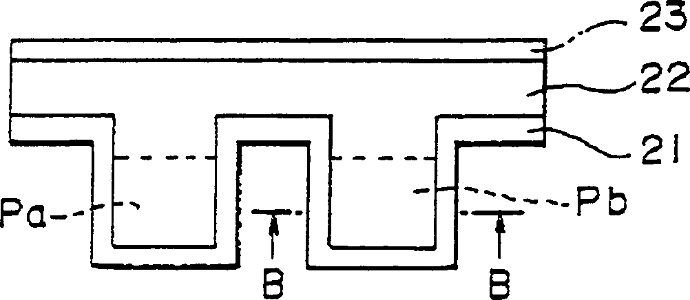
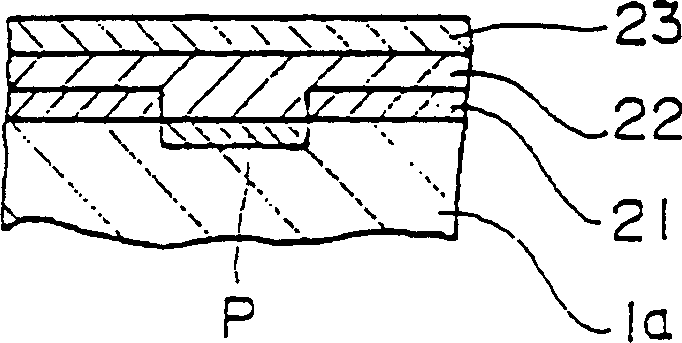
[0026] The following is an explanation of related embodiments of a semiconductor device and its manufacturing method proposed according to the present invention. FIG. 1 is a schematic diagram illustrating a first embodiment. Just as shown in the schematic plan view in FIG. 1(a), the semiconductor device of the first embodiment has an LOC structure, and is provided with an on-chip semiconductor element 1, and a plurality of pins L and common lines 2a and 2b pass through the semiconductor element 1. The insulating tape T on the substrate 1a is connected to provide electrical connections for the electrode pads that handle common signals among the many electrode pads on the substrate 1a, and the bonding wire W that electrically connects the electrode pads to the pin L.
[0027] In this semiconductor device, the common line 2a constitutes a power line by being electrically connected to the electrode pad P1 connected to the power supply, and the common line 2b constitutes a ground w...
PUM
 Abstract
Description
Claims
Application Information