Pulse generator circuit

A technology of pulse generation circuit and circuit, applied in the direction of pulse processing, pulse shaping, pulse technology, etc., to achieve the effect of strong ability

Inactive Publication Date: 2004-04-28
RENESAS ELECTRONICS CORP
View PDF0 Cites 0 Cited by
  • Summary
  • Abstract
  • Description
  • Claims
  • Application Information

AI Technical Summary

Problems solved by technology

Since this circuit is usually composed of inverters connected in multiple stages, there is a disadvantage

Method used


Image

  • Pulse generator circuit
  • Pulse generator circuit
  • Pulse generator circuit

Examples


Example Embodiment

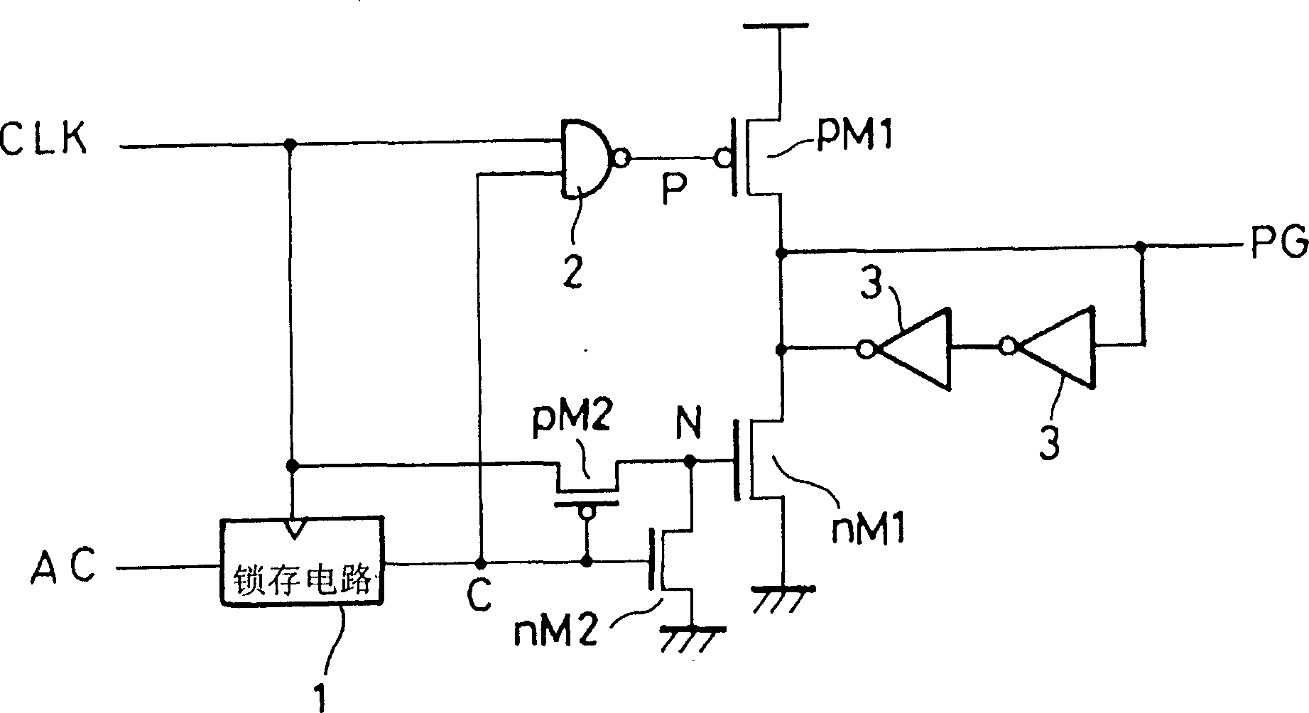
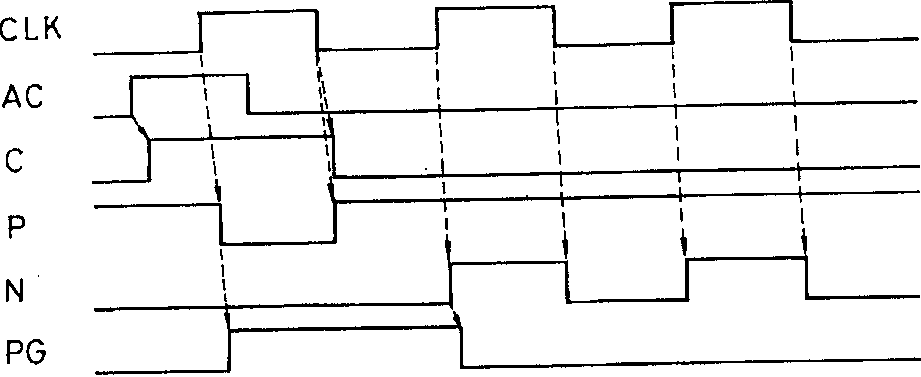
[0024] Hereinafter, embodiments of the present invention will be specifically described with reference to the drawings. figure 1 Is a circuit diagram showing a pulse generating circuit of an embodiment of the present invention, figure 2 It is a timing chart of the circuit operation.

[0025] The operation start signal AC and the clock signal CLK are input to the latch circuit 1, and a signal C that rises when the signal AC is high (burst start signal) and falls when the clock signal CLK falls. Therefore, the latch circuit 1 generates a signal C that expands the high level of AC (burst start signal) to the lower edge of CLK.

[0026] The output C of the latch circuit 1 is input to the gates of the n-type MOS transistor nM2 and the p-type MOS transistor pM2. In addition to inputting the clock signal CLK to the latch circuit 1, it is also input to the NAND circuit 2 and the transistor pM2. The output C of the latch circuit 1 is input to the other input terminal of the NAND circuit ...


PUM


Abstract

The invention provides a kind of pulse generation circuit which could produce the pulse with high speed and fixed pulse-width and could produce the pulse of the activating basic pulse PG which is suitable for the reading and writing motion from the internal of the synchronized integrated circuit, in particular the semiconductor memory circuit. Said pulse PG makes the transistor pM1 conduct by way of catering the high fringe of the first cycle in the timer clock CLK to produce start fringe, and makes the transistor nM1 conduct by way of catering the high fringe of the second cycle in the timer clock CLK to produce the end fringe of PG. Thus, the time period until producing the pulse is high speed. Since the pulse width is determined by the period, it is not changed completely.

Description

Technical field [0001] The present invention relates to a pulse generating circuit that generates a basic pulse for activating internal read and write operations of a synchronous integrated circuit such as a semiconductor memory circuit, and more particularly to a pulse generating circuit that uses two or more cycles to perform an internal access operation mode. Background technique [0002] Figure 8 It is a circuit diagram showing a conventional pulse generating circuit, Picture 9 Indicates its timing chart. In the latch circuit 20, the internal activation information generated by the operation start signal AC is latched according to the clock signal CLK, and at the same time, the output of the latch circuit 20 and the NAND logic of the clock signal CLK are obtained to generate the information expanded to the lower edge of CLK. Internal signal A. Furthermore, in the NOR circuit 22, the short pulse signal B synchronized with the upper edge of the clock signal CLK is generated ...

Claims


Application Information

Patent Timeline
IPC IPC(8): G06F1/04G06F1/06H03K5/04H03K5/1534
CPCH03K5/1534
Inventor 高桥弘行
Owner RENESAS ELECTRONICS CORP
Why Eureka
Try Eureka