Optical elements and method for fabricating the same

Active Publication Date: 2020-01-16
VISERA TECH CO LTD
View PDF6 Cites 0 Cited by
  • Summary
  • Abstract
  • Description
  • Claims
  • Application Information

AI Technical Summary

Benefits of technology

[0022]In the present invention, it is not required that a microlens (ML) structure be disposed over the color filters. Light is conducted into photodiode (PD) areas through a wave-guiding element which is fabricated on metal grids. The present invention provides a two-step process for fabricating a wave-guiding structure. A first organic layer (refractive index: about 1.4 to about 1.55) is first formed between the metal grids. The first organic layer is used as a buffer layer for a subsequent etching process. A second organic layer (refractive index: about 1.2 to about 1.45) is then formed on the first organic layer and the metal grids. The second organic layer is used to form the wave-guiding element. When a first etching process is performed using, for example, haloalkyl gas as an etching gas, the second organic layer is etched but the first organic layer is left. The remaining first organic layer is then removed by a second etch

Problems solved by technology

Since the conditions (e.g. gas type and etching time) of the etching process are hard to c

Method used


Image

  • Optical elements and method for fabricating the same
  • Optical elements and method for fabricating the same
  • Optical elements and method for fabricating the same

Examples


Embodiment Construction

[0033]The following description is of the best-contemplated mode of carrying out the invention. This description is made for the purpose of illustrating the general principles of the invention and should not be taken in a limiting sense. The scope of the invention is best determined by reference to the appended claims.

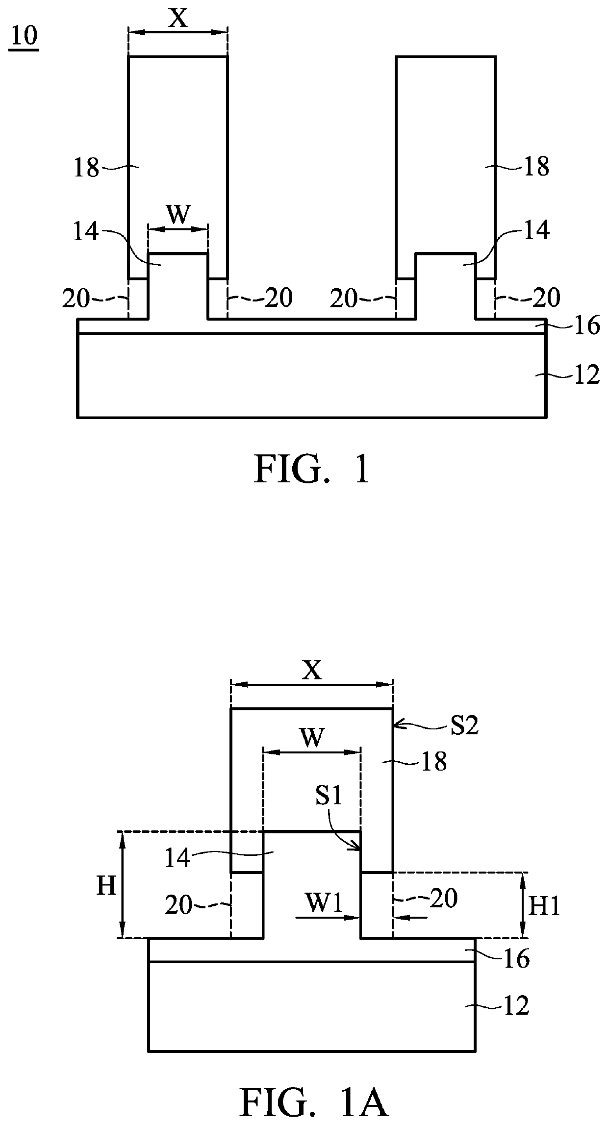
[0034]Referring to FIG. 1, in accordance with one embodiment of the invention, an optical element 10 is provided. FIG. 1 shows a cross-sectional view of the optical element 10.

[0035]The optical element 10 comprises a substrate 12, a plurality of metal grids 14, an oxide layer 16, and a plurality of organic layers 18. The plurality of metal grids 14 are formed on the substrate 12. The oxide layer 16 is formed on the substrate 12 between the plurality of metal grids 14. The plurality of organic layers 18 are formed on the plurality of metal grids 14. The width X of the organic layer 18 is greater than the width W of the metal grid 14. Specifically, a gap 20 is formed bet...


PUM


Abstract

A method for fabricating an optical element is provided. The fabrication method includes the following steps. A substrate is provided. A plurality of metal grids are formed on the substrate. A first organic layer is formed on the substrate between the plurality of metal grids. A second organic layer is formed on the first organic layer and the plurality of metal grids. The second organic layer and the first organic layer are etched to leave the plurality of metal grids and a plurality of patterned second organic layers on the plurality of metal grids. An optical element fabricated by the method is also provided.

Description

BACKGROUND OF THE INVENTIONField of the Invention[0001]The invention relates to a fabrication method of an optical element, and more particularly to a fabrication method of an optical element using a two-step wave-guiding process, and an optical element fabricated thereby.Description of the Related Art[0002]In a conventional process for fabricating a wave-guiding structure, after metal grids are formed on a substrate, a guiding film is coated over the metal grids and the substrate. A mask layer is then formed on the guiding film. An etching process is performed on the guiding film until the substrate is exposed. Since the conditions (e.g. gas type and etching time) of the etching process are hard to control properly, the substrate often suffers from being damaged during the etching process.[0003]Therefore, development of a simple fabrication method of an optical element which is capable of preventing damage to the substrate during the etching process is desirable.BRIEF SUMMARY OF TH...

Claims


Application Information

Patent Timeline
IPC IPC(8): B05D5/06B05D7/00B05D7/14B05D3/10
CPCB05D7/5483G02B5/201B05D7/14B05D5/06B05D3/107G02B6/136G02B6/122G02B5/3058G02B6/1221H01L21/0475H01L21/311H01L21/28H01L21/3065H01L21/30604
Inventor CHENG, SHENG-CHUANCHEN, HUANG-JENLIN, CHI-HANWU, HAN-LIN
Owner VISERA TECH CO LTD
Why Eureka
Try Eureka