Formation method of semiconductor structure

A technology of semiconductors and structural materials, applied in the manufacture of semiconductor/solid-state devices, electrical components, circuits, etc., can solve the problems of poor shape of adjacent patterns and the inability of adjacent patterns to be formed, and achieve good shape of patterns and exposure effect. Good results

Pending Publication Date: 2022-07-29
SEMICON MFG INT (SHANGHAI) CORP +1
View PDF0 Cites 0 Cited by
  • Summary
  • Abstract
  • Description
  • Claims
  • Application Information

AI Technical Summary

Problems solved by technology

[0004] However, with the further improvement of the integration of semiconductor structures, the distance between two adjacent design patterns needs to be further reduced, and the size of the distance exceeds the limit of the existing photolithography process, or is close to the existing photolithography process limit, leading to the fact that adjacent patterns with small pitches cannot be formed, or the morphology of many adjacent patterns with small pitches is poor

Method used


Image

  • Formation method of semiconductor structure
  • Formation method of semiconductor structure
  • Formation method of semiconductor structure

Examples


Embodiment Construction

[0025] As described in the background art, with the further improvement of the integration of semiconductor structures, it is necessary to further reduce the spacing between two adjacent design patterns, and the size of the spacing exceeds the limit of the existing lithography process, or is close to the existing Due to the limitation of the lithography process, adjacent patterns with small spacing cannot be formed, or the appearance of many adjacent patterns with small spacing is poor. The following will be described in detail with reference to the accompanying drawings.

[0026] It should be noted that the "surface" in this specification is used to describe the relative positional relationship in space, and is not limited to whether it is in direct contact.

[0027] Figure 1 to Figure 5 It is a schematic structural diagram of each step of a method for forming a semiconductor structure.

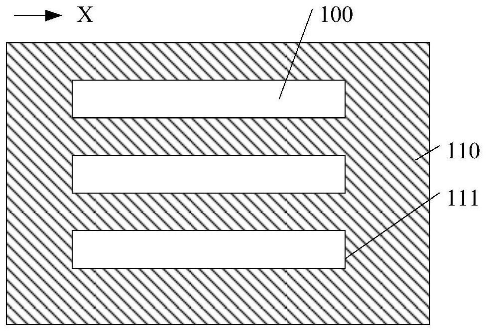
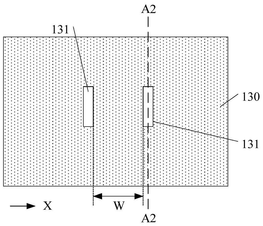
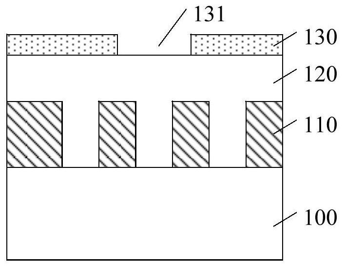
[0028] Please refer to figure 1 , providing the layer to be etched 100; forming a sa...


PUM


Abstract

A method for forming a semiconductor structure comprises the following steps: providing a layer to be etched; a first sacrificial layer is formed on the surface of the to-be-etched layer, a first opening extending in the first direction is formed in the first sacrificial layer, and the first opening exposes the surface of the to-be-etched layer; forming an initial second sacrificial layer on the first sacrificial layer and in the first opening; forming an initial first mask layer on the surface of the initial second sacrificial layer; a plurality of patterning steps are carried out on the initial first mask layer to form a first mask layer, a plurality of partition mask openings distributed in the first direction are formed in the first mask layer, each partition mask opening stretches across the first opening in the second direction, and the second direction is perpendicular to the first direction. Therefore, adjacent patterns with small spacing and good morphology can be transmitted to the to-be-etched layer.

Description

technical field [0001] The present invention relates to the field of semiconductor manufacturing, in particular to a method for forming a semiconductor structure. Background technique [0002] With the improvement of circuit integration and the increase of scale, the size of the unit device in the circuit continues to shrink, and the requirements for the integrated circuit manufacturing process continue to increase. high. [0003] With the continuous reduction of the design size, the minimum resolution of the design pattern has exceeded the limit capability of the existing optical lithography platform. The industry has adopted a variety of technical solutions to solve this technical problem. According to the international semiconductor technology blueprint, Double patterning technology (DPT), extreme ultraviolet technology (EUV), electron beam direct writing (EBL) and other technical solutions have been placed high hopes by the industry. [0004] However, with the further ...

Claims


Application Information

Patent Timeline
IPC IPC(8): H01L21/027
CPCH01L21/0274
Inventor 高宗朋何欣祥胡敏达
Owner SEMICON MFG INT (SHANGHAI) CORP
Why Eureka
Try Eureka