Supercharge Your Innovation With Domain-Expert AI Agents!

Photoresist removal process and semiconductor manufacturing process

A photoresist and process technology, used in semiconductor/solid-state device manufacturing, electrical components, circuits, etc., can solve problems such as substrate damage, and achieve the effect of improving manufacturing efficiency and product yield

Active Publication Date: 2022-07-29
度亘激光技术(苏州)有限公司
View PDF26 Cites 0 Cited by
  • Summary
  • Abstract
  • Description
  • Claims
  • Application Information

AI Technical Summary

Problems solved by technology

[0003]However, in the above-mentioned semiconductor manufacturing process, when the residual photoresist is removed by hydrogen-containing gas such as ammonia, the ambient temperature is usually kept at a relatively high temperature, and it is not necessary to The temperature is lower than 290°C, so the substrate needs to be in a high-temperature and high-proportion hydrogen-containing gas environment for a long time, which makes the substrate easy to damage

Method used


Image

  • Photoresist removal process and semiconductor manufacturing process
  • Photoresist removal process and semiconductor manufacturing process
  • Photoresist removal process and semiconductor manufacturing process

Examples


Embodiment

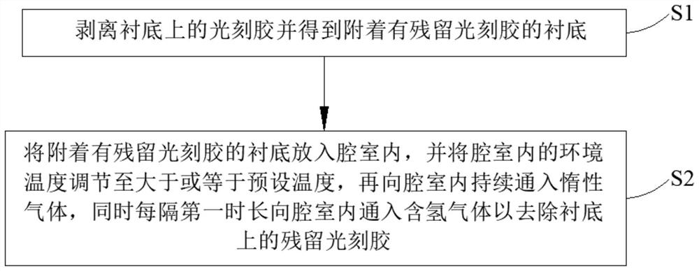
[0031] like figure 1 As shown, the photoresist removal process provided by this embodiment includes:

[0032] Step S1: peel off the photoresist 2 on the substrate 1 and obtain the substrate 1 with the residual photoresist attached;

[0033] Step S2: Put the substrate 1 with the residual photoresist attached into the chamber, and adjust the ambient temperature in the chamber to be greater than or equal to the preset temperature, and then continue to introduce an inert gas into the chamber, while every first The hydrogen-containing gas is passed into the chamber for a long time to remove the residual photoresist 2 on the substrate 1 .

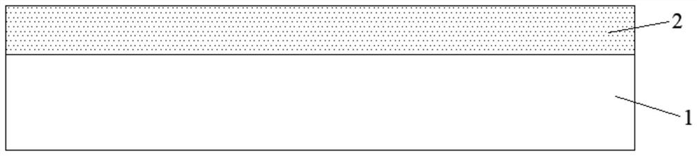
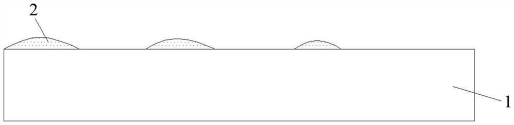
[0034] In the photoresist removal process provided in this embodiment, step S1 is first performed to peel off the photoresist 2 on the substrate 1 of the semiconductor. After step S1, as follows figure 2 and image 3 As shown, most of the photoresist 2 on the substrate 1 is peeled off, but there is still residual photoresist 2 . Wherein, in ...


PUM


Abstract

The invention provides a photoresist removal process and a semiconductor manufacturing process, and relates to the technical field of semiconductor manufacturing processes. The photoresist removal process comprises the following steps: stripping photoresist on a substrate and obtaining the substrate attached with residual photoresist; and putting the substrate attached with the residual photoresist into a chamber, adjusting the environment temperature in the chamber to be greater than or equal to a preset temperature, continuously introducing inert gas into the chamber, and introducing hydrogen-containing gas into the chamber every first time so as to remove the residual photoresist on the substrate. According to the photoresist removal process provided by the invention, the residual photoresist can be effectively removed by utilizing the environment temperature which is greater than or equal to the preset temperature (the preset temperature can be 290-310 DEG C) and the hydrogen-containing gas, and the hydrogen-containing gas is intermittently introduced; the photoresist can be removed, meanwhile, the substrate can be prevented from being damaged due to the fact that the substrate is continuously located in a high-temperature and high-proportion hydrogen-containing gas environment for a long time, and then the product yield can be increased.

Description

technical field [0001] The invention relates to the technical field of semiconductor manufacturing processes, in particular to a photoresist removal process and a semiconductor manufacturing process. Background technique [0002] When manufacturing semiconductors, the existing manufacturing process is usually to coat a photoresist on the substrate first, then expose the substrate to develop the photoresist, and then use a dry or wet method to etch out a mask pattern, and then peel off photoresist. When stripping the photoresist, the photoresist is usually removed by spraying high-pressure NMP (N-methylpyrrolidone, abbreviated as NMP). However, this method cannot completely remove the photoresist, so after stripping the photoresist, It is also necessary to use a hydrogen-containing gas such as ammonia gas to remove the remaining photoresist. After removing the remaining photoresist, the substrate after removing the photoresist is coated in a PECVD (Plasma Enhanced Chemical ...

Claims


Application Information

Patent Timeline
IPC IPC(8): H01L21/027H01L21/033
CPCH01L21/0272H01L21/0331
Inventor 于良成惠利省杨国文
Owner 度亘激光技术(苏州)有限公司
Features
  • R&D
  • Intellectual Property
  • Life Sciences
  • Materials
  • Tech Scout
  • Unparalleled Data Quality
  • Higher Quality Content
  • 60% Fewer Hallucinations
Learn More