Supercharge Your Innovation With Domain-Expert AI Agents!

Contact improved test head between contact probe and guide hole

A technology of test head and guide hole, which is applied in the field of test head, can solve the problems of frequency performance limitation of test head, impossible to ensure effective electrical connection between probe and metallized part, and overall performance limitation of test head

Pending Publication Date: 2022-07-29
TECHNOPROBE
View PDF0 Cites 0 Cited by
  • Summary
  • Abstract
  • Description
  • Claims
  • Application Information

AI Technical Summary

Problems solved by technology

[0009] However, it is notoriously often impossible to ensure an effective electrical connection between the probe tip and the metallization, leading to an unacceptable limitation in the overall performance of the test head
In other words, it is not always possible to ensure proper sliding contact between the contact probe and the wall of the guide hole, so that the frequency performance of the test head is often limited

Method used


Image

  • Contact improved test head between contact probe and guide hole
  • Contact improved test head between contact probe and guide hole
  • Contact improved test head between contact probe and guide hole

Examples


Embodiment Construction

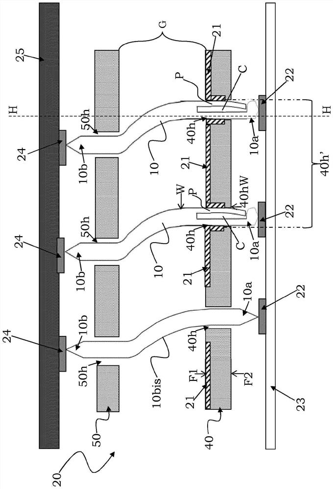
[0036] With reference to these drawings, especially figure 1 An example of a test head according to the invention is generally indicated schematically at 20 .

[0037] Notably, the figures are schematic and not to scale, but are drawn to emphasize important features of the invention. Furthermore, in the drawings, various elements are depicted schematically, the shapes of which vary depending on the desired application. It should also be noted that in the figures, the same reference numbers refer to elements that are identical in shape or function. Finally, certain features described in relation to the embodiments shown in the figures also apply to other embodiments shown in other figures.

[0038] The test head 20 is adapted to be connected to equipment (not shown) for testing electronic devices (eg high frequency devices) integrated on the semiconductor wafer 23 .

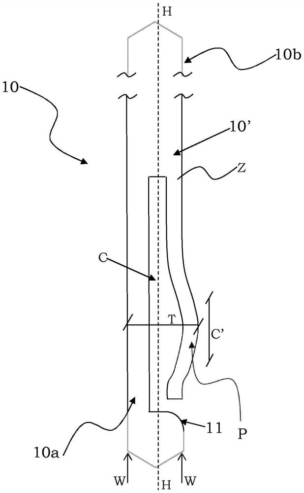
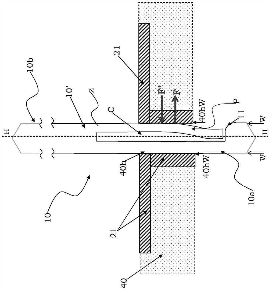
[0039] The test head 20 includes a plurality of contact probes 10 slidably received in the test head for con...


PUM


Abstract

A test head (20) for testing the functionality of an electronic device comprises: a plurality of contact probes (10, 10bis) comprising probe bodies (10 ') extending longitudinally between respective ends (10a, 10b) adapted to contact respective contact pads; at least one lower guide (40) provided with a guide hole (40h) for slidably receiving the contact probe (10, 10bis); and a conductive portion (21) in the lower guide (40), the conductive portion (21) comprising at least one set of holes (40h ') of the guide holes (40h) and being adapted to contact and short-circuit a corresponding set of contact probes (10) housed in the set of holes (40h') for carrying a specific type of signal. Suitably, at least the contact probe (10) housed in the set of holes (40h ') comprises an elastically deformable portion (P) adapted to be at least partially inserted into the set of guide holes (40h'), wherein the portion (P), when received in the set of guide holes (40h '), is in a configuration that deforms due to contact with at least one wall (40hW) of the guide holes and exerts a reaction force (F) on the wall (40hW) to ensure sliding contact during testing of the electronic device.

Description

technical field [0001] The present invention relates to a test head, which is suitable for testing electronic devices integrated on a semiconductor wafer. The following description is only made with reference to the application field, and its sole purpose is to simplify its description. Background technique [0002] As is well known, a test head is essentially a device suitable for connecting a plurality of contact pads of a microstructure (in particular an electronic device integrated on a semiconductor wafer) with its functional test (in particular electrical test, or general test) ) is electrically connected to the corresponding channel of the test device. [0003] Testing of integrated circuits is particularly useful for detecting and isolating defective circuits as early as the production stage. Therefore, test heads are often used to test circuits integrated on wafers before they are diced and assembled into chip packages. [0004] The test head essentially comprises...

Claims


Application Information

Patent Timeline
IPC IPC(8): G01R1/073G01R1/067
CPCG01R1/07357G01R1/06738G01R1/07314G01R1/06716G01R1/06761G01R1/073
Inventor 罗伯特·克里帕
Owner TECHNOPROBE
Features
  • R&D
  • Intellectual Property
  • Life Sciences
  • Materials
  • Tech Scout
  • Unparalleled Data Quality
  • Higher Quality Content
  • 60% Fewer Hallucinations
Learn More