

Testing of semiconductor device and fabrication process of semiconductor device
A semiconductor and tester technology, applied in semiconductor/solid-state device testing/measurement, electronic circuit testing, instruments, etc., can solve problems such as inability to accurately test semiconductor devices, and achieve the effect of accurate testing
- Summary
- Abstract
- Description
- Claims
- Application Information
AI Technical Summary
Problems solved by technology
Method used
Image

Examples
no. 1 example
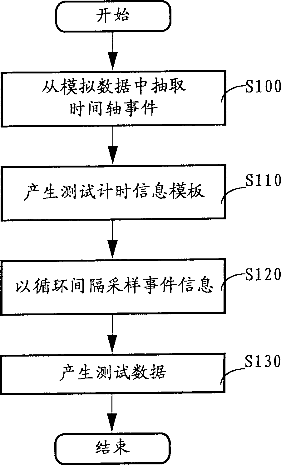
[0059] FIG. 3 shows the structure of a semiconductor test system according to a first embodiment of the present invention.
[0060] Referring to Fig. 3, the semiconductor test system of the present embodiment comprises a test data processor 11 and a tester 19 for testing an integrated circuit 18 together with the test data processor 11, wherein the test data processor 11 includes storing analog data produced by an external simulator. storage device 12. The test data processor 11 also includes a central processing unit (CPU) 13 cooperating with the storage device 12 , wherein the test data processor 11 also includes an event information buffer 14 , a timing information buffer 15 , a cycle counter 16 and a test buffer 17 . It should be noted that the structure of Figure 3 may be implemented by any suitable platform, including engineering workstations or personal computers.
[0061] In the structure of FIG. 3 , test data is provided from the test data processor 11 to the tester ...
no. 2 example
[0081] A second embodiment of the present invention addressing the compatibility between simulation accuracy and tester accuracy for testing integrated circuits will be described below with reference to FIG. 7 . The second embodiment also relates to verification of uncertain events. In this embodiment, it should be noted that the structure of the test system used is the same as that of the test system in FIG. 3 . Therefore, a description of the test system will be omitted.
[0082] Referring to Fig. 7, Fig. 7 has represented the flow chart of the process that CPU 13 is carried out, and process starts from step S20 corresponding to step S10 of Fig. S24. After step S24, proceed to step S25. In step S25, verification processing is performed on events that cannot be verified by the accuracy of the tester 19. Such events are called indeterminate events.
[0083] It should be noted that the process of FIG. 7 is provided in the form of computer readable program codes and stored in...
no. 3 example
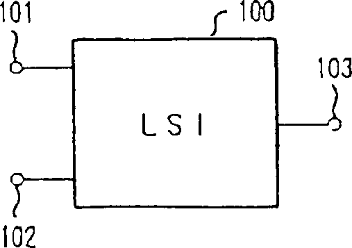
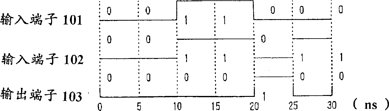
[0098] The verification of the input / output dead zone will be described below with reference to FIG. 10 to illustrate the semiconductor test system according to the third embodiment of the present invention. is generated when it is in the input state, wherein those previously described components in FIG. 10 are indicated by the same reference numerals, and their descriptions are omitted.
[0099] 10, in addition to the storage device 12, the CPU 13, the timing information buffer 15, the cycle counter 16 and the test data buffer 17, the semiconductor test system also includes a first event information buffer 25, a second event information buffer 26 and The third event information buffer 27 . In this embodiment, the integrated circuit to be tested is capable of changing the state of the output terminal 23 between an input state and an output state.
[0100] FIG. 11 is a flowchart showing operations performed by the CPU in the system of FIG. 10 . It should be noted that the pro...
PUM
 Abstract
Description
Claims
Application Information