Drive transistor sructure for ink jet print head chip its making process

A technology for driving transistors and inkjet print heads, which is applied in semiconductor/solid-state device manufacturing, printing, semiconductor devices, etc., and can solve problems such as increased parasitic resistance, high wafer manufacturing costs, and increased heat

Inactive Publication Date: 2005-06-15
宇临科技股份有限公司
View PDF0 Cites 0 Cited by
  • Summary
  • Abstract
  • Description
  • Claims
  • Application Information

AI Technical Summary

Problems solved by technology

Although the miniaturization of MOSFET components can provide more drive transistors per unit area, but the miniaturization of components will increase the parasitic resistance of MOSFET components and other circuits, and the heat generated per unit area will also increase, requiring higher costs. Wafer Manufacturing Cost

Method used


Image

  • Drive transistor sructure for ink jet print head chip its making process
  • Drive transistor sructure for ink jet print head chip its making process
  • Drive transistor sructure for ink jet print head chip its making process

Examples


Embodiment Construction

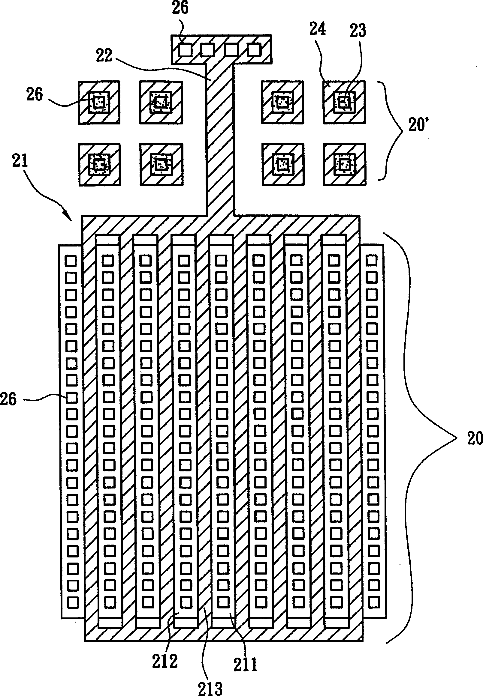
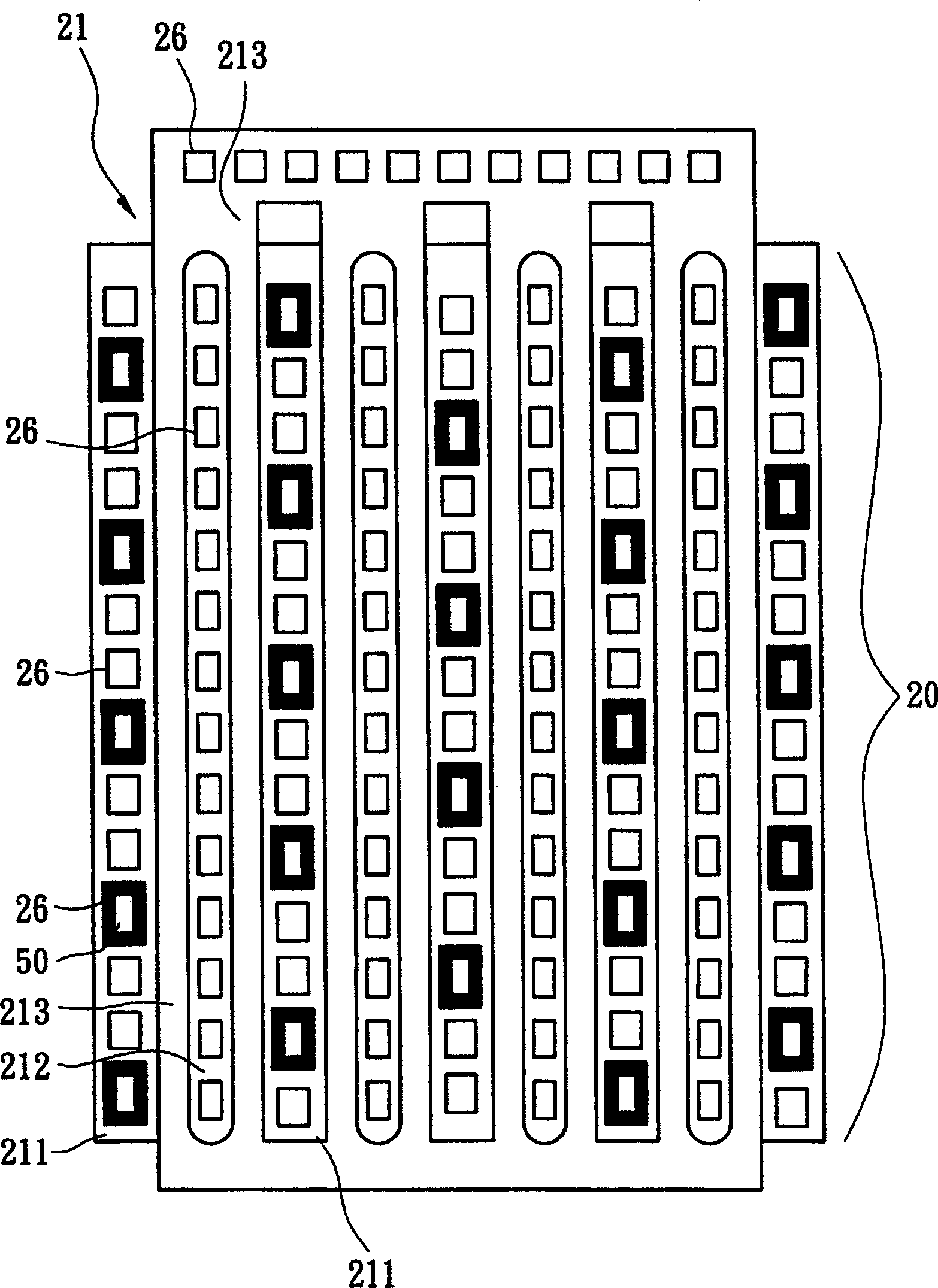
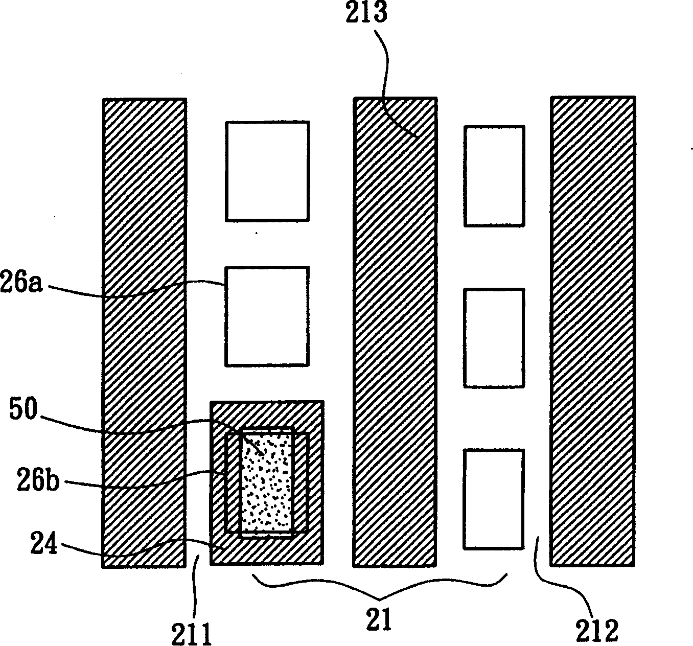
[0020] refer to Figure 2A , which is a schematic top view of the drive transistor structure of the inkjet print head chip according to an embodiment of the present invention, showing a structure layout of the drive transistor with the base embedded in the source (BES). A plurality of bases 50 are disposed in the active region 20 of the drive transistor structure, and the active region 20 has a plurality of MOSFET elements 21 connected in parallel. Each MOSFET element includes: a source region 211 , a drain region 212 and a gate 213 . The plurality of base electrodes 50 are arranged in the source region 211 at a proper distance. Appropriate contact holes 26 are formed on the source region 211 , the drain region 212 , the gate 213 and the base 50 . Since the MOSFET element 21 adopts a design with a large channel width to length ratio, that is, the channel width is much greater than the channel length. Usually, the active region 20 has a width of more than 400 microns. The g...


PUM


Abstract

A kind of structure and manufacturing method of the driving transistor of inkjet printing head chip, a plurality of bases are widely distributed in the source electrode of a large-area metal oxide semiconductor field effect transistor (MOSFET) active region, make MOSFET channel to The equivalent resistance between the bases (R 8 ) is greatly reduced as the distance decreases, thus avoiding the occurrence of secondary breakdown; in addition, since the base is set in the active region, there is no need to pre-define the field oxide layer outside the active region Therefore, this driving transistor structure can save about 20% of occupied area and reduce the average production cost of each wafer.

Description

technical field [0001] The invention relates to a driving circuit of an inkjet printing head, in particular to a driving transistor structure of an inkjet printing head wafer of an integrated driving circuit and a manufacturing method thereof. Background technique [0002] An inkjet printer is a common computer peripheral device, and usually has an inkjet printhead for ejecting ink droplets, such as a thermal bubble inkjet printhead. The basic structure of a general inkjet print head usually includes: an ink channel, an orifice for ink ejection and an orifice sheet, an excitation element for ejecting ink, and an appropriate driving circuit. When the inkjet printer is printing, the ink is excited by the excitation element (for example, the heating body) to be ejected from the nozzle holes on the nozzle sheet, and ink dots can be generated on the paper. Generally speaking, a thermal bubble inkjet print head uses a resistor as an ink excitation device to heat the ink in the in...

Claims


Application Information

Patent Timeline
Patent Type & Authority Patents(China)
IPC IPC(8): B41J2/14H01L21/336H01L29/78
Inventor 刘建宏刘健群张智超胡纪平陈俊融
Owner 宇临科技股份有限公司
Why Eureka
Try Eureka