Dry-process deep-etching silicon miero mechanical working method an glass substrate

A technology of silicon micromachines and glass substrates, applied in the direction of microstructure technology, microstructure devices, manufacturing microstructure devices, etc., can solve the problems of lower processing yield, lower performance, and difficult control, etc., and achieve low manufacturing costs and finished products High efficiency, easy operation and manufacturing

Inactive Publication Date: 2006-07-05
MT MICROSYST
View PDF0 Cites 0 Cited by
  • Summary
  • Abstract
  • Description
  • Claims
  • Application Information

AI Technical Summary

Problems solved by technology

In the silicon-based process, the surface processing adopts a multi-layer thin film structure (generally less than 3 μm) and sacrificial layer corrosion technology. The production process is complicated and difficult to control. At present, there are few domestic applications. The bulk silicon process is mainly used, and the bulk silicon process is used most. The most important is the bulk silicon melting process, that is, the double-layer structure of silicon-glass bonding. Compared with the surface process, the bulk silicon process has a larger processing space (generally greater than 20 μm), but the traditional bulk silicon melting process requires a long time and high temperature. Diffusion of concentrated boron, which will bring greater stress to the device and cause structural deformation and performance degradation of the device. In addition, the traditional bulk silicon melting process requires special equipment to thin and polish the chip, which will make the processing The yield rate is greatly reduced, and the traditional bulk silicon melting process also requires a toxic wet etching process that is harmful to humans, so the traditional bulk silicon melting process has many shortcomings

Method used


Image

  • Dry-process deep-etching silicon miero mechanical working method an glass substrate
  • Dry-process deep-etching silicon miero mechanical working method an glass substrate

Examples


Embodiment Construction

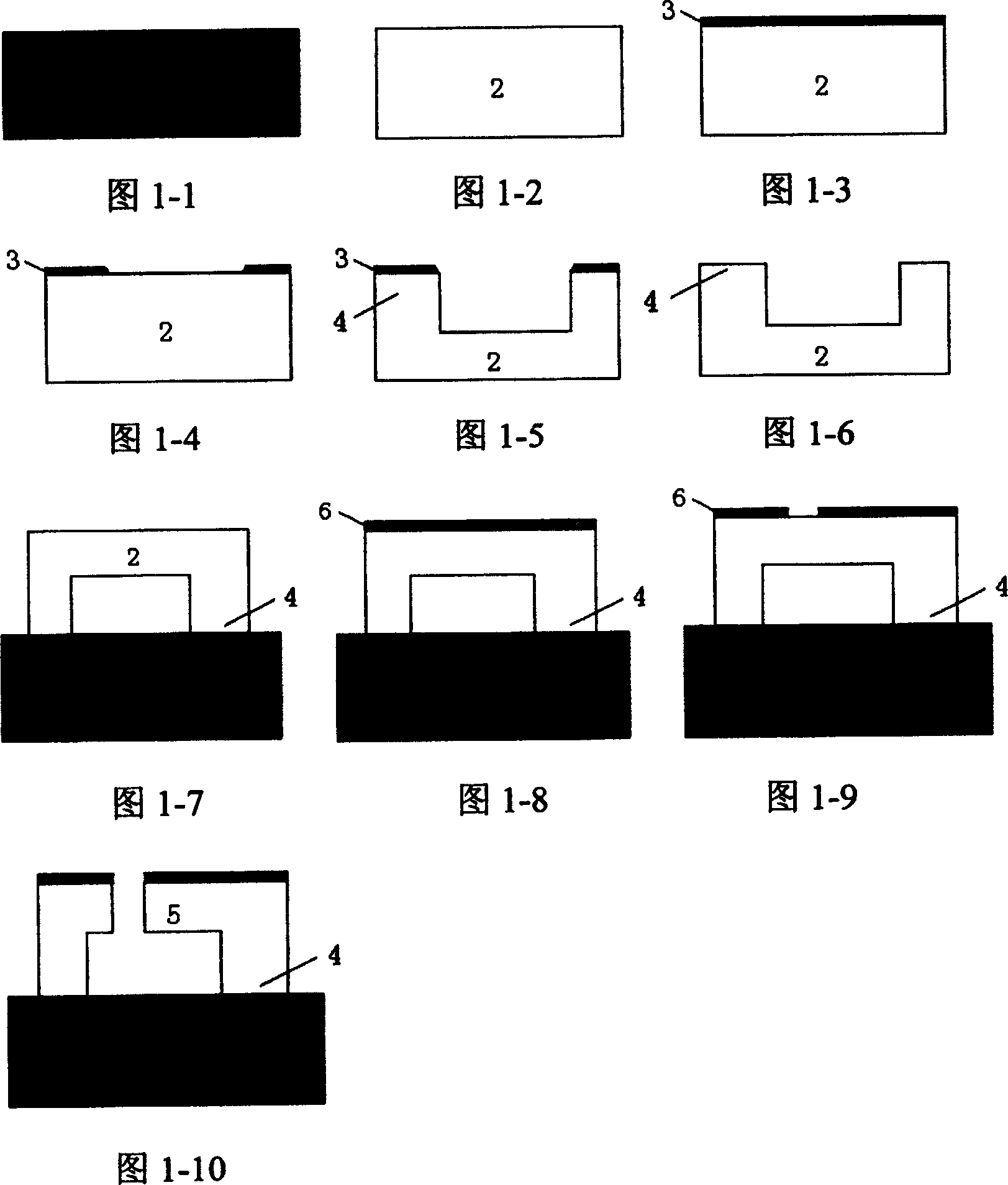
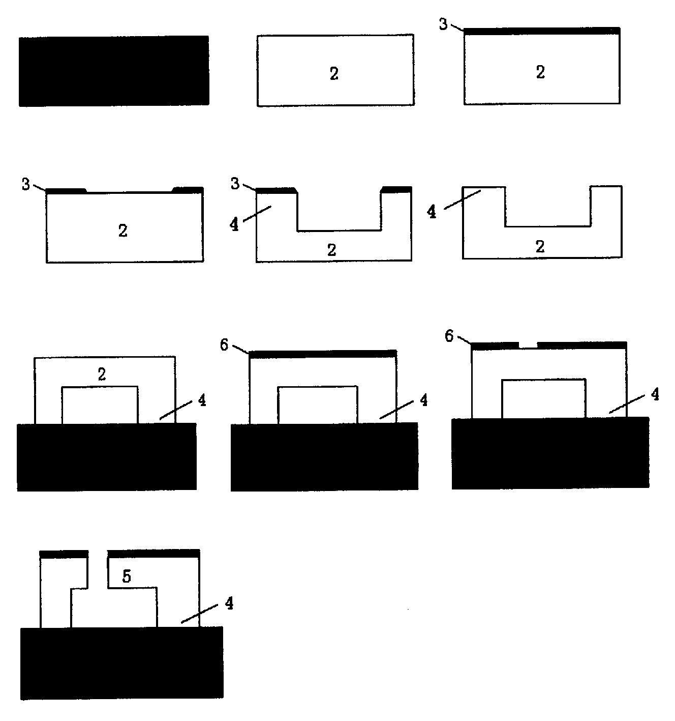
[0020] (1) Double-sided polishing heat-resistant 7740 glass sheet 1 on a commercially available general polishing machine, such as Picture 1-1 .

[0021] (2) double-sided polished single crystal silicon wafer 2 on a commercially available general polishing machine, the thickness of double-sided polished single crystal silicon wafer 2 is 280 μ m to 320 μ m, and the thickness of embodiment double-sided polished single crystal silicon wafer 2 is 300 μ m, such as figure 1 -2.

[0022] (3) A layer of positive AZ1450 photoresist 3 is coated on the double-sided polished single crystal silicon wafer 2, and the thickness of the coated photoresist 3 is 2 μm, such as figure 1 -3.

[0023] (4) Carry out lithography with a commercially available general-purpose lithography machine, and form a silicon-glass bonded bonding table 4 pattern window on one side of the double-sided polished single crystal silicon wafer 2, such as figure 1 -4.

[0024] (5) With the photoresist 3 as a mask, de...


PUM

PropertyMeasurementUnit
thicknessaaaaaaaaaa
depthaaaaaaaaaa

Abstract

The invention discloses a tiny mechanical process method for glass substrate with whole-dry deep carved silicon. It uses double-surface photoetching, deep reaction ion etching and silicon-glass bonding technology; it realizes the movable suspending microstructure produce with low stress and big longitudinal size on the glass substrate. The invention is low cost and easy to be operated; the rate of finished products is high.

Description

technical field [0001] The invention relates to a micro-machining method for fully dry deep etching silicon on a glass substrate in the technical field of micro-electro-mechanical processing, and is especially suitable for the manufacture of various movable micro-electro-mechanical structural devices with low stress and large longitudinal dimensions . Background technique [0002] Micro-electro-mechanical system, also known as MEMS, refers to a controllable and movable micro-electromechanical device with a size below the millimeter level. The combination of these constitutes a system with specific functions, which has the advantages of light weight, small size, low cost and integration. MEMS technology emerged in the mid-1980s and developed rapidly in the early 1990s. At present, many developed countries in the world have given priority to the development of MEMS technology. The United States lists MEMS technology, aerospace technology and information technology as the th...

Claims


Application Information

Patent Timeline
Patent Type & Authority Patents(China)
IPC IPC(8): B81C1/00
Inventor 徐永青何洪涛罗蓉
Owner MT MICROSYST
Why Eureka
Try Eureka