Supercharge Your Innovation With Domain-Expert AI Agents!

Method for driving plasma display panel

A plasma display and drive waveform technology, applied in the direction of static indicators, instruments, color TV components, etc., can solve the problems of unable to turn on the unit that must be turned on, redundant, AY wall voltage reset failure rate increase, etc.

Inactive Publication Date: 2006-12-20
HITACHI CONSUMER ELECTRONICS CORP
View PDF1 Cites 0 Cited by
  • Summary
  • Abstract
  • Description
  • Claims
  • Application Information

AI Technical Summary

Problems solved by technology

This results in an increase in the rate at which the AY wall voltage fails to reset
PDP will encounter problems such as opening redundant units or failing to open units that must be opened.

Method used


Image

  • Method for driving plasma display panel
  • Method for driving plasma display panel
  • Method for driving plasma display panel

Examples


no. 1 example

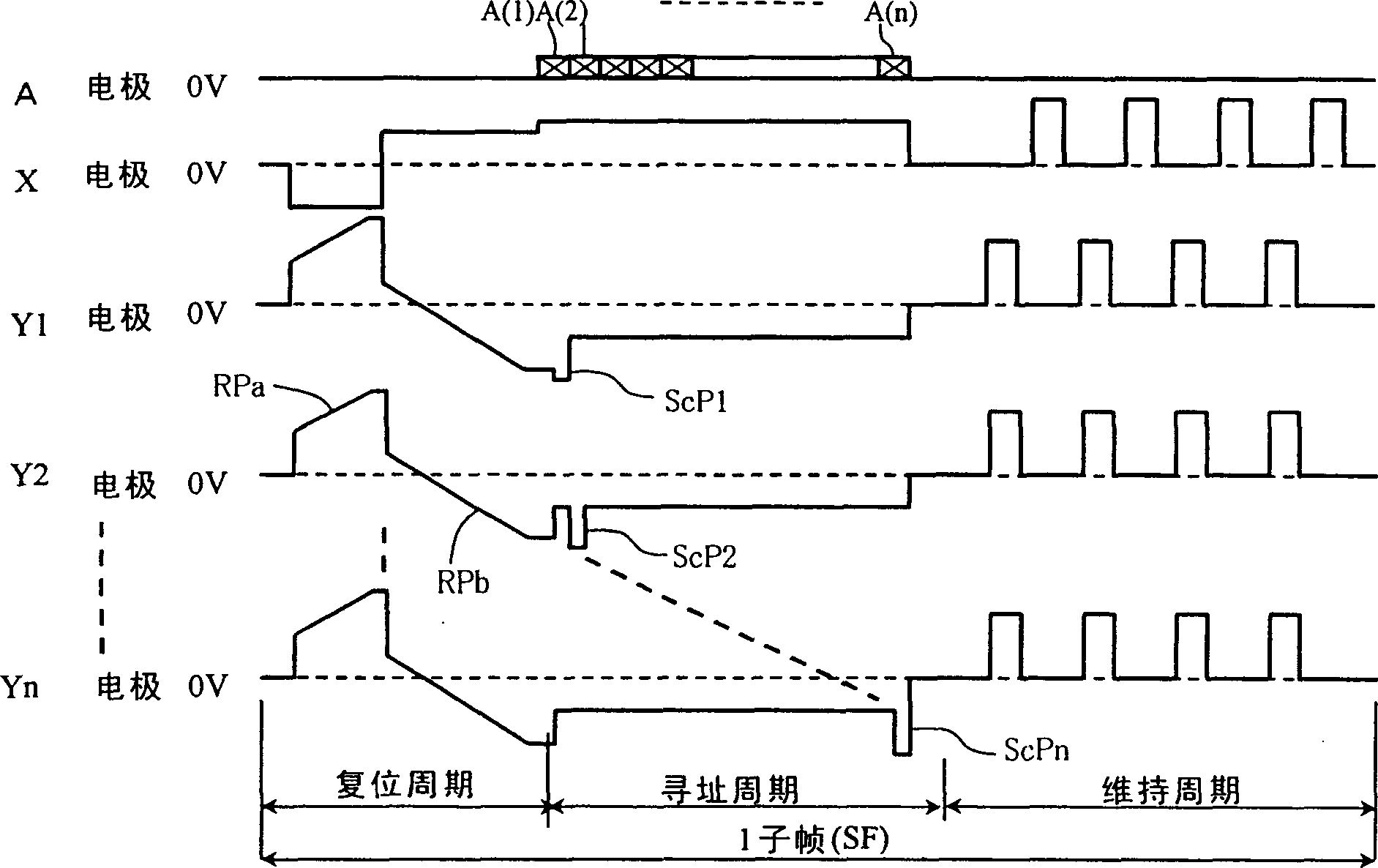
[0143] Reference Figure 16 , The driving waveform and the reset condition formula according to the first embodiment of the present invention will be described.

[0144] In the first embodiment, in the sustain period, ±V S A pulse train of / 2 is applied to the X electrode and the Y electrode, and the potential of the A electrode is fixed at the ground potential. Consider the voltage between the electrodes, ±V S The alternating waveform is applied between the X electrode and the Y electrode, ±V S An alternating waveform of / 2 is applied between the A electrode and the Y electrode. In the sustain period, the bias voltage of the AY applied voltage (ie, the AY wall voltage) is zero.

[0145] The reset condition formula according to the first embodiment is:

[0146] 2V tAY -V tXY ≤V YR -V XR .

[0147] Because the discharge threshold voltage V tAY The general value of is approximately 200V, and the discharge threshold voltage V tXY The general value of is approximately 230V, so the fol...

no. 2 example

[0153] Reference Figure 17 , The driving waveform and the reset condition formula according to the second embodiment of the present invention will be described.

[0154] From 0 to V S The sustain driving waveform composed of alternating pulses is applied to the X electrode and the Y electrode, and the potential of the address electrode is fixed to zero. The voltage amplitude V applied to the X electrode when the ramp wave is applied to the X electrode in the second step of resetting the waveform XR And the voltage amplitude applied to the Y electrode -V YR When the following reset conditions are met:

[0155] 2V tAY -V tXY ≤V YR -V XR +V S

[0156] "Simultaneous reset guarantee area" and "maintain operation line" accord with Figure 15 (a) The relationship in.

[0157] As in the first embodiment, the general settings are as follows:

[0158] 2V tAY -V tXY= 170.

[0159] By setting the following formula to 170V or greater:

[0160] V YR -V XR +V S

[0161] "XY and AY discharge a...

no. 3 example

[0165] Reference Figure 18 , The driving waveform and the reset condition formula according to the third embodiment of the present invention will be described. The sustain driving waveform in the third embodiment is considered to be a waveform based on the driving waveform in the first embodiment, and it has several pulses at the end of the sustain period, that is, the sustain pulse of the second embodiment is applied.

[0166] The sustain drive pulse will be ±V immediately before the end of the sustain period s1 / 2 alternating pulse is applied to the X electrode and Y electrode, and will change from 0 to V until the end of the sustain period s2 The alternating pulse is applied to the X electrode and Y electrode. The potential of the address electrode is set to zero.

[0167] The amplitude of the voltage applied to the X electrode when the ramp wave is applied to the X electrode through the second step of the reset waveform V XR And the voltage amplitude applied to the Y electrod...


PUM


Abstract

A method of driving a PDP including alternately-arranged X and Y electrodes and A electrodes crossing the X and Y electrodes provides a recurring cycle of a resetting period, an addressing period, and a sustaining period. The method includes applying a ramp waveform in the resetting period. Discharge starting threshold voltages between the X and Y electrodes and between the A and Y electrodes are denoted by VtXY and VtAY, respectively. Voltages applied between the X and Y electrodes and between the A and Y electrodes at the trailing edge of the ramp waveform are denoted by VXY and VAY, respectively. An offset voltage of the voltage applied between the A and Y electrodes at the end of the sustaining period is denoted by Vaoff. In such a case, the voltage of a driving waveform for each electrode is set so as to satisfy the relational expression '2VtAY-VtXY<=2VAY-VXY-2Vaoff'.

Description

Technical field [0001] The present invention relates to a method of driving a plasma display, and more specifically, the present invention relates to an improvement of a driving method of reset. Background technique [0002] figure 1 The structure of a plasma display (hereinafter referred to as PDP (Plasma display panel)) is shown. [0003] The PDP is manufactured by connecting the front substrate 10 and the rear substrate 20 to each other. The front substrate 10 includes a plurality of display electrode pairs (X electrodes 11 and Y electrodes 12). The dielectric layer 13 covers these electrodes, and the protective film 14 made of MgO or the like covers the dielectric layer 13. [0004] A plurality of address electrodes (A electrodes 21) are arranged on the rear substrate 20. The dielectric layer 23 covers the A electrode 21. A barrier 25 that divides the discharge space into a plurality of regions is provided between adjacent A electrodes 21. Each area uses one of a red fluore...

Claims


Application Information

Patent Timeline
Patent Type & Authority Patents(China)
IPC IPC(8): G09G3/28H04N5/66G09G3/10G09G3/20G09G3/288G09G3/291G09G3/292G09G3/294G09G3/298G09G3/299
CPCG09G3/2927G09G3/296
Inventor 崎田康一
Owner HITACHI CONSUMER ELECTRONICS CORP
Features
  • R&D
  • Intellectual Property
  • Life Sciences
  • Materials
  • Tech Scout
  • Unparalleled Data Quality
  • Higher Quality Content
  • 60% Fewer Hallucinations
Learn More