Once write film storage

A technology of memory unit and memory element, applied in the direction of static memory, read-only memory, digital memory information, etc., can solve the problem that EPROM and fuse programmable devices are not easy to integrate, and MRAM and polymer memory devices do not provide high density and low Voltage characteristics and other issues

Inactive Publication Date: 2002-04-17
SAMSUNG ELECTRONICS CO LTD
View PDF1 Cites 6 Cited by
  • Summary
  • Abstract
  • Description
  • Claims
  • Application Information

AI Technical Summary

Problems solved by technology

But EPROM and fuse programmable devices do not offer the high density and low voltage characteristics of MRAM and polyme

Method used


Image

  • Once write film storage
  • Once write film storage
  • Once write film storage

Examples


Embodiment Construction

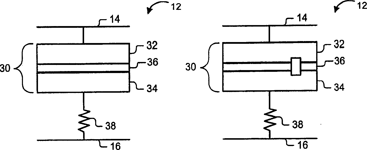
[0018] As shown in the drawings for purposes of illustration, the invention is embodied in a data storage device comprising an array of thin film memory cells and circuitry for reading and writing the memory cells. A write operation may be performed by damaging the thin film isolation layers of at least some of the memory cells.

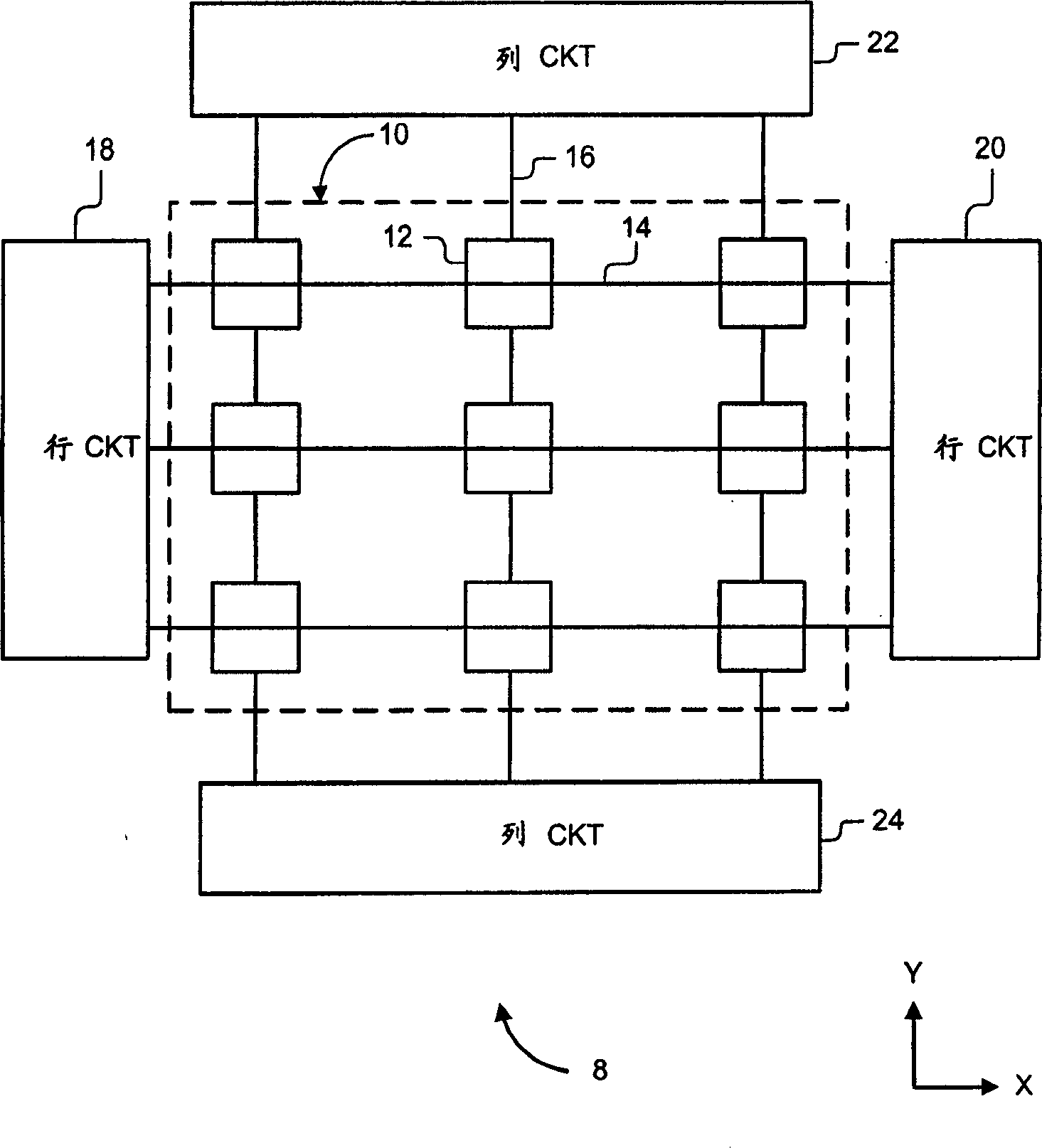
[0019] refer to figure 1 , which illustrates a data storage device 8 comprising a resistive cross-point array 10 of thin film memory cells 12 . The memory cells 12 are arranged in rows and columns, the rows extending in the x direction and the columns extending in the y direction. To simplify the explanation of device 8, only a relatively small number of memory cells 12 are shown. Arrays of virtually any size can be used.

[0020] Traces serving as word lines 14 run in-plane along the x-direction on one side of the array 10 . Traces serving as bitlines 16 run in-plane along the y-direction on the other side of the array 10 . There may be one wor...


PUM


Abstract

A data storage device (8, 210, 310) includes a group of memory cells (12, 110, 312) and write-once operations may be performed by damaging the thin-film barriers (36) of at least some of the memory cells (12, 110, 312). The data storage device (8, 210, 310) may be a Magnetic Random Access Memory ('MRAM') device.

Description

technical field [0001] The present invention relates to data storage devices. In particular, the present invention relates to write-once thin film data storage devices. Background technique [0002] New classes of non-volatile thin film memory include random access magnetic memory ("MRAM") based on spin-dependent tunneling ("SDT") junctions. A typical SDT junction has a pinned ferromagnetic layer, a sensing ferromagnetic layer, and a thin insulating tunnel isolation layer sandwiched between the ferromagnetic layers. A logic value can be written to the SDT junction by applying a magnetic field to set the magnetization orientation of the SDT junction either parallel (logic value "0") or antiparallel (logic value "1"). The relative orientation and spin polarization of the ferromagnetic layers determine the resistance state (R or R+ΔR) of the SDT junction. The logic value stored in the SDT junction can be read by detecting the resistance of the SDT junction. [0003] Another...

Claims


Application Information

Patent Timeline
IPC IPC(8): G11C13/00G11C11/14G11C11/15
CPCG11C17/146G11C11/14G11C11/15
Inventor F·A·佩尔纳T·C·安东尼
Owner SAMSUNG ELECTRONICS CO LTD
Why Eureka
Try Eureka