A kind of black phosphorene thin film memory and its preparation method

A technology of black phosphorene and memory, which is applied in the field of memory, can solve the problems of insufficient research and development, and achieve the effect of fast transformation speed and stable read and write voltage

Active Publication Date: 2018-12-04
GRIMAT ENG INST CO LTD
View PDF5 Cites 0 Cited by
  • Summary
  • Abstract
  • Description
  • Claims
  • Application Information

AI Technical Summary

Problems solved by technology

Black phosphorene has excellent properties, but as a new type of material, its research and development is not deep enough, especially in the field of storage. Therefore, it is an important technological progress in this field to provide a storage device based on black phosphorene thin film

Method used


Image

  • A kind of black phosphorene thin film memory and its preparation method
  • A kind of black phosphorene thin film memory and its preparation method
  • A kind of black phosphorene thin film memory and its preparation method

Examples


Embodiment 1

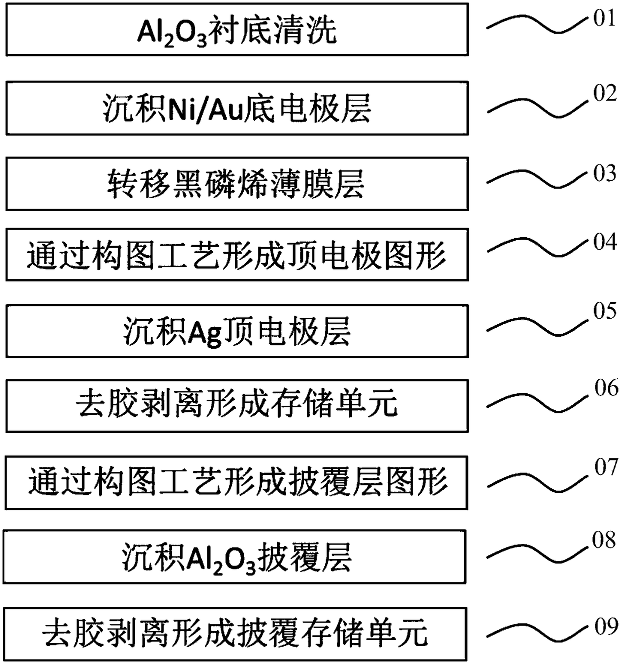
[0040] figure 2 The flow chart of this embodiment for preparing a black phosphorene thin film memory through a photolithography patterning process includes:

[0041] (01)Al 2 O 3 Substrate cleaning

[0042] (02) Depositing a Ni / Au bottom electrode layer;

[0043] (03) Transfer the black phosphorene film to obtain a black phosphorene film layer;

[0044] (04) Forming a top electrode pattern through a photolithography patterning process;

[0045] (05) Depositing the Ag top electrode layer;

[0046] (06) Degumming and peeling technology to form a storage unit;

[0047] (07) Form the cladding layer pattern by photolithography patterning process;

[0048] (08) Deposit Al 2 O 3 Cladding layer

[0049] (09) Gluing and peeling to form a covered storage unit.

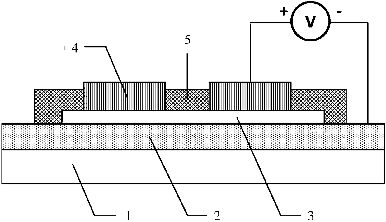
[0050] The basic structure of black phosphorene thin film memory is obtained as figure 1 As shown, it includes a substrate 1, a bottom electrode 2, a black phosphorene film layer 3 and a top electrode 4 in order from bottom to top, wherein th...


PUM

PropertyMeasurementUnit
thicknessaaaaaaaaaa
thicknessaaaaaaaaaa
thicknessaaaaaaaaaa

Abstract

The present invention relates to a black phosphorene film memory and a preparation method thereof. The preparation method of the black phosphorene film memory comprises the following steps: (1) cleaning a substrate; (2) forming a bottom electrode on the substrate; (3) forming the black phosphorene film layer on the bottom electrode; (4) forming the graph of a top electrode on the black phosphorene film layer through a composition process; (5) forming the top electrode on the black phosphorene film layer, and obtaining a memory unit; (6) forming the graph of a cladding layer at the upper side of the memory unit through the composition process; and (7) finally forming the cladding layer to allow the cladding layer to coat the part of the black phosphorene film layer without being coated with the top electrode, and obtaining the memory. The black phosphorene film memory is rapid in the transforming speed and stable in read-write voltage.

Description

Technical field [0001] The invention belongs to the technical field of memory, and particularly relates to a black phosphorene film memory and a preparation method thereof. Background technique [0002] According to the International Semiconductor Technology Roadmap (ITRS) forecasts on the development trend of the integrated circuit field, by 2020, the feature size of integrated circuits will be reduced to less than 10 nanometers, so that traditional devices will face a series of technical and physical limits. challenge. At this time, new materials need to be introduced to solve many problems that traditional devices cannot solve. Two-dimensional crystals are nanometer-thick planar crystals stacked by several monoatomic layers. They have unique electrical, optical, and magnetic properties, and have their own unique structural advantages. Therefore, common two-dimensional materials such as graphene, Silylene, molybdenum disulfide and black phosphorene have all received extensive...

Claims


Application Information

Patent Timeline
Patent Type & Authority Patents(China)
IPC IPC(8): H01L27/105
CPCH01L27/105
Inventor 赵鸿滨屠海令张国成魏峰杨志民姚俊奇
Owner GRIMAT ENG INST CO LTD
Why Eureka
Try Eureka