
Wide-area single-photon detector with time-gating capability

a single-photon detector and wide-area technology, applied in the field of photodetectors, can solve the problems of not being able to achieve fast time-gating capability, and achieve the effects of reducing the complexity of time-domain diffuse optics, wide active area, and improving signal harvesting

Pending Publication Date: 2022-03-03
POLITECNICO DI MILANO +1
View PDF0 Cites 2 Cited by
  • Summary
  • Abstract
  • Description
  • Claims
  • Application Information

AI Technical Summary

Benefits of technology

The present invention provides a photodetector with single-photon sensitivity, wide photosensitive area, and fast time-gating capability at the same time. The detector has two photosensitive devices, which maximize the photosensitive area, or fill-actor. This allows for faster and more efficient detection of light.

Problems solved by technology

On the other side, SiPMs may have a wide active area, as discussed in document “Fast silicon photomultiplier improves signal harvesting and reduces complexity in time-domain diffuse optics” cited above, but are not suitable for fast time-gating capability, because of their high stray capacitance and the presence of the integrated quenching resistor, both preventing fast transitions of their bias voltage, needed for rapidly turning ON the detector.

Method used


Image

  • Wide-area single-photon detector with time-gating capability
  • Wide-area single-photon detector with time-gating capability
  • Wide-area single-photon detector with time-gating capability

Examples


Embodiment Construction

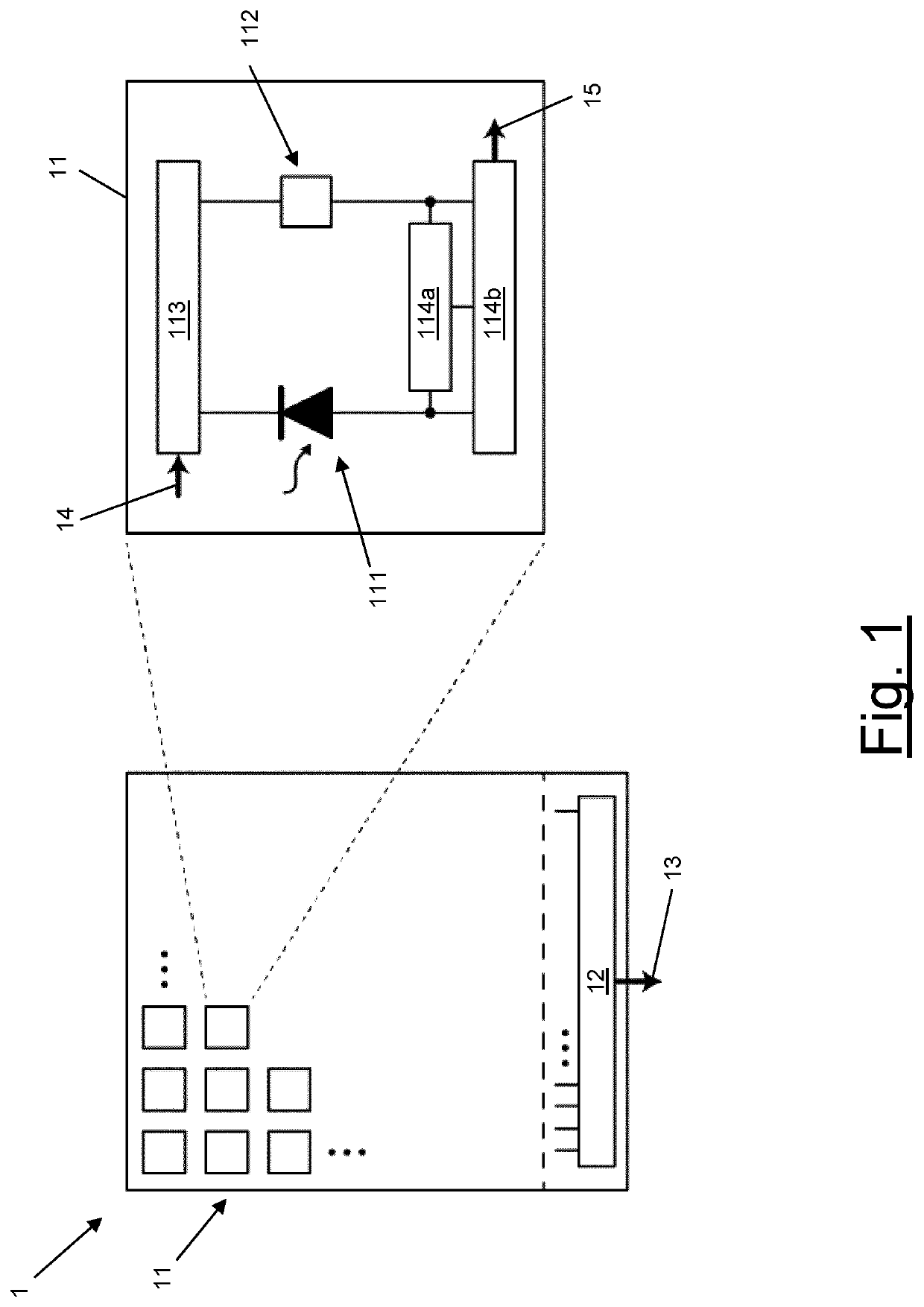
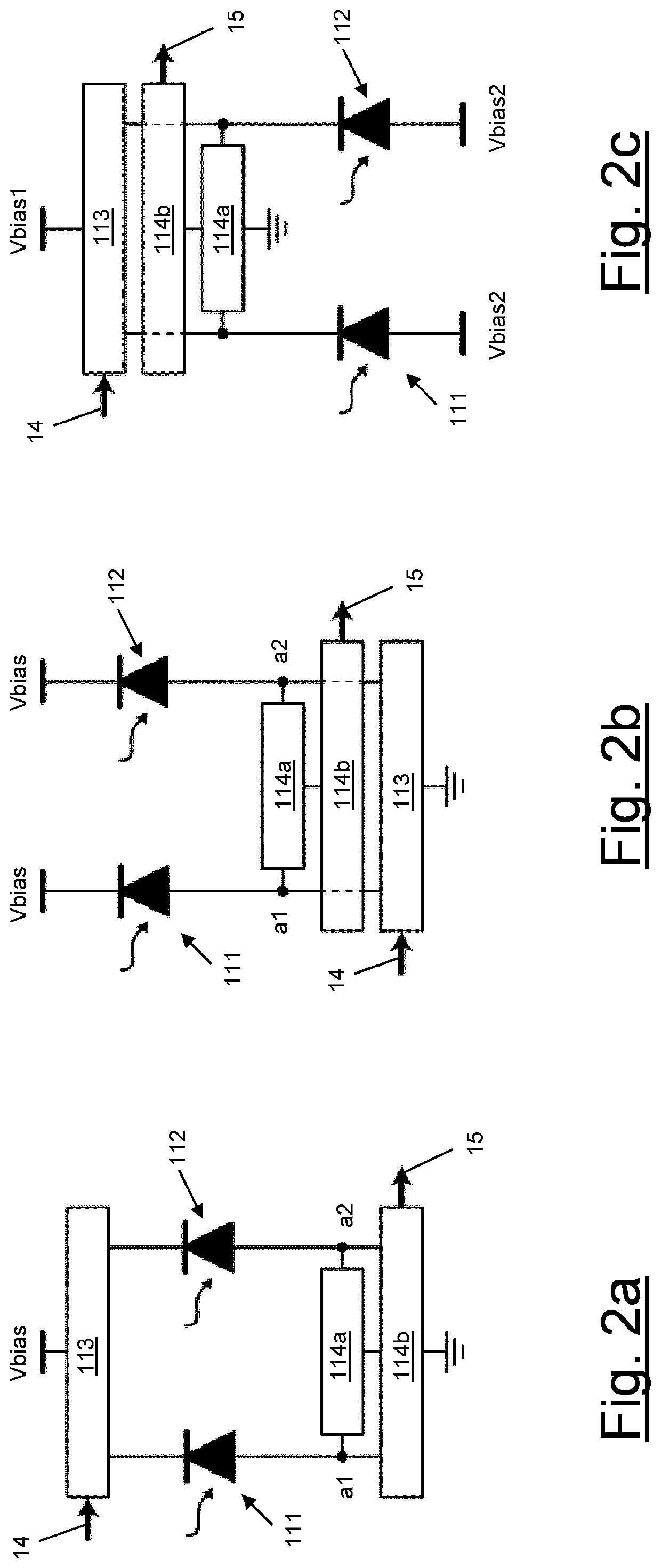
[0053]FIG. 1 schematically shows a photodetector 1 according to an embodiment of the present invention. FIG. 1 also shows an enlarged view of a microcell 11 of the photodetector 1 according to a possible implementation thereof.

[0054]According to the present invention, the photodetector 1 is a solid-state photodetector that can be fabricated on one or more semiconductor substrates by using any one of the currently available microelectronic technologies, such as any standard or customized CMOS or BCD processing in silicon, and / or SiGe, and / or III-V semiconductors, or a fully-custom recipe, either monolithically fabricated or also using 3D stacking (e.g. wafer-to-wafer bonding, chip-to-chip bonding, or System-on-Chip assembly) or a multiplicity of them.

[0055]The photodetector 1 preferably comprises a bi-dimensional array of M×N microcells 11, where M and N are integer numbers ≥1. In the photodetector 1 according to the present invention, the microcells 11 are laid out side-by-side acco...


PUM


Abstract

A photodetector may include an array of microcells and an output module configured to collect, from each microcell, an output signal indicative of a photon detection and to combine the collected output signals in at least one output line. Each microcell comprises a first device and a second device, wherein at least one of the devices is a photosensitive device capable of detecting the photon; a time-gating module connected to said at least one photosensitive device and configured to provide a gate signal to the at least one photosensitive device to activate it; and a readout module configured to receive, upon arrival of the photon on the at least one activated photosensitive device, a corresponding signal from the at least one activated photosensitive device and, on the basis of the received signal, to provide the output signal to the output module.

Description

TECHNICAL FIELD[0001]The present invention relates to the field of photodetectors, in particular solid-state single-photon detectors, and even more particularly single-photon detectors having time-gating capabilities and a wide photosensitive area.BACKGROUND ART[0002]Diffuse optics is the study of photon propagation in highly scattering media.[0003]Among the applications of diffuse optics, Near-Infrared Spectroscopy (NIRS) is used to estimate the composition and microstructure of biological tissues and other highly scattering media, down to a depth of few centimetres, by estimating the optical absorption and scattering properties of the sample. The estimation may be performed through NIRS, by means of either continuous wave (CW-NIRS), or pulsed (time-domain or time-resolved TD-NIRS), or sine wave modulated (frequency-domain or frequency-resolved FD-NIRS) light excitation.[0004]NIRS can be exploited for functional brain imaging, muscle oxygenation monitoring, cancer detection, fruit ...

Claims


Application Information

Patent Timeline
Patent Type & Authority Applications(United States)
IPC IPC(8): H01L31/107G01S17/894G01S7/4863G01S17/18H01L27/146H04N25/00
CPCH01L31/107G01S17/894H01L27/14643G01S17/18G01S7/4863H04N25/773
Inventor TOSI, ALBERTOVILLA, FEDERICA ALBERTAZAPPA, FRANCOTORRICELLI, ALESSANDRODALLA MORA, ALBERTOCONTINI, DAVIDEPIFFERI, ANTONIO GIOVANNITARONI, PAOLADI SIENO, LAURABUTTAFAVA, MAUROCONCA, ENRICOSCROFANI, GABRIELETISA, SIMONE
Owner POLITECNICO DI MILANO
Learn More