Method and apparatus for optically analyzing a surface

a surface and optical analysis technology, applied in the field of interferometric devices and methods for optical analysis of surfaces, can solve the problems of inability to provide information about the surface topography, slow measurement process, and difficulty in obtaining an ideal flat top surface for metal and insulators, and achieve the effect of facilitating non-contact analysis of surfaces quickly and efficiently

Inactive Publication Date: 2007-04-26
PHASE SHIFT TECH
View PDF17 Cites 185 Cited by
  • Summary
  • Abstract
  • Description
  • Claims
  • Application Information

AI Technical Summary

Benefits of technology

[0013] Accordingly, an object of the present invention is to provide apparatu...

Problems solved by technology

The CMP process exhibits material- and geometry-dependent removal rates, leading to difficulties in obtaining an ideally flat top surface for metal and insulator.
Furthermore, the measurement process is slow because it is inherently a single-point measurement where profiles or two-dimensional maps have to be built up sequentially.
The film thickness is measured using spectrophotometers o...

Method used


Image

  • Method and apparatus for optically analyzing a surface
  • Method and apparatus for optically analyzing a surface
  • Method and apparatus for optically analyzing a surface

Examples


Embodiment Construction

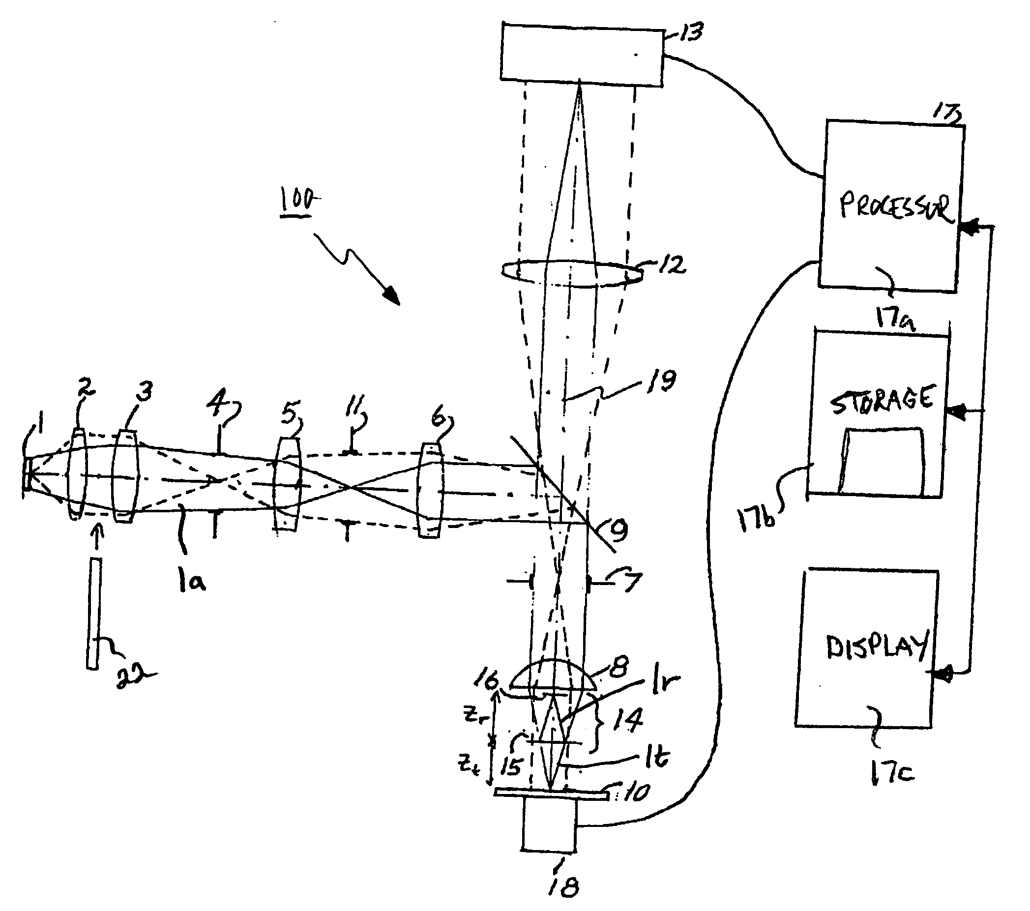
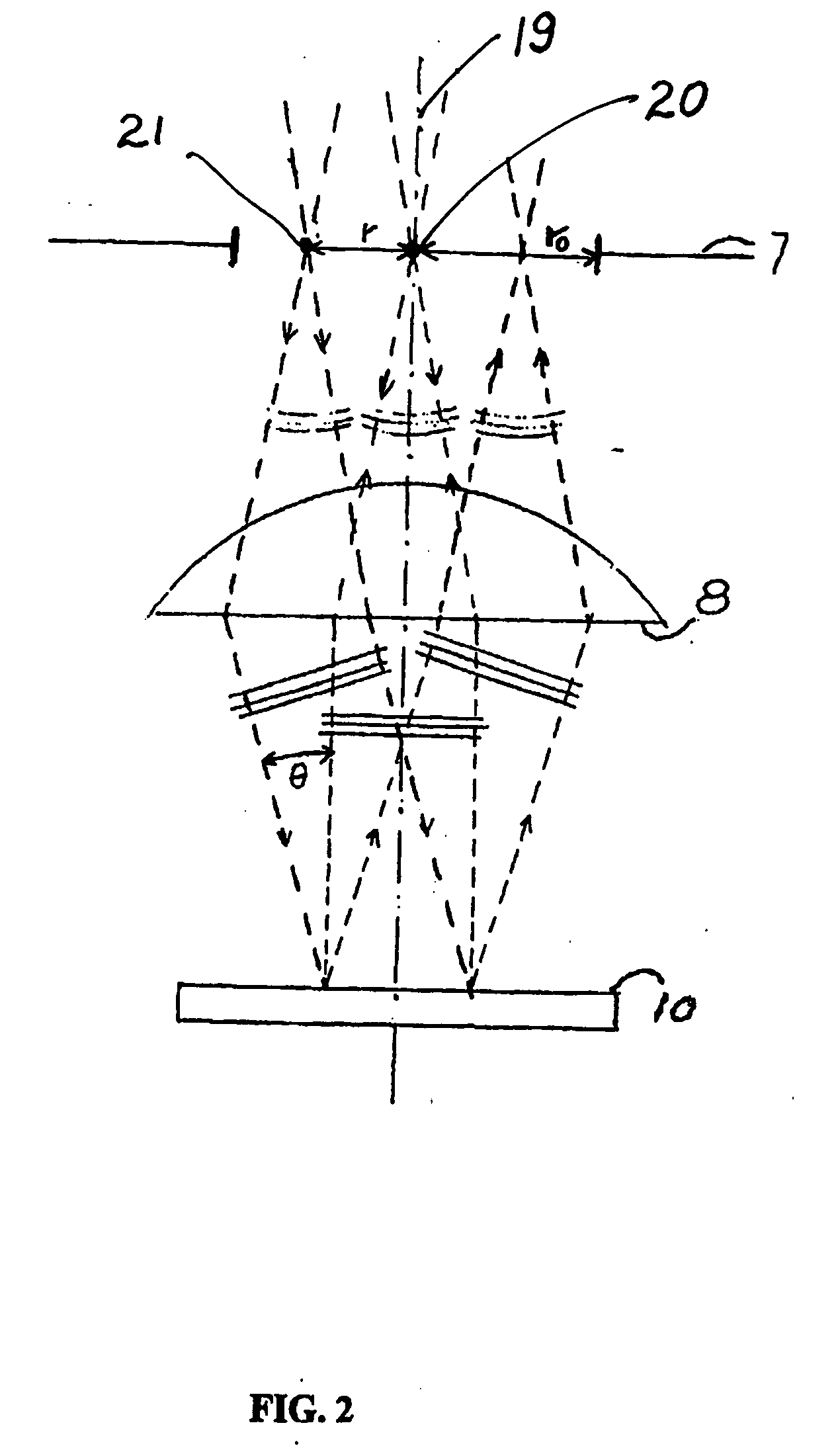
[0095] Reference will now be made in detail to the presently preferred embodiments and methods of the invention as illustrated in the accompanying drawings, in which like reference characters designate like or corresponding parts throughout the drawings. It should be noted, however, that the invention in its broader aspects is not limited to the specific details, representative devices and methods, and illustrative examples shown and described in this section in connection with the preferred embodiments and methods. The invention according to its various aspects is particularly pointed out and distinctly claimed in the attached claims read in view of this specification, and appropriate equivalents.

[0096] The embodiments and methods of this invention are useful for optically analyzing test objects, also referred to herein as test pieces, and more preferably the surfaces of test objects, particularly at high magnifications or resolutions. Examples of test objects would include, witho...


PUM


Abstract

Apparatus and methods are provided for analyzing surface characteristics of a test object using broadband scanning interferometry. Test objects amenable to these apparatus and methods include but are not limited to semiconductor wafers, semiconductor devices, metallic surfaces, and the like. An interferometry system is used to obtain an interferometry signal and related to data embodied in the signal representative of the test object surface. This signal and/or data is used to construct an n-dimensional function that includes an independent frequency variable and an independent time variable, and/or an n-dimensional function that includes an independent scale variable and an independent time variable, and/or a multi-domain function. These functions are compared with various models to obtain a best match that is then used to characterize the test object surface.

Description

BACKGROUND OF THE INVENTION [0001] 1. Field of the Invention [0002] The present invention relates to interferometric devices and methods for optically analyzing surfaces, for example, such as the surfaces of semiconductor wafers, semiconductor devices, magnetic surfaces, and the like. [0003] 2. Description of the Related Art [0004] Interferometers are commonly used for testing the shape and topography of surfaces. Good interferometers have height sensitivity in the sub-nanometer range, providing two-dimensional maps in rapid, non-contact operation. A large variety of optical interferometer configurations exist, as well as processing techniques to derive surface topography maps from the measured interferogram intensities. [0005] The fringes of the interferogram are governed by the phase difference between a test beam and a reference beam. The phase of the test beam includes a propagation phase delay and a phase shift on reflection at the surface of a test object or test piece. While ...

Claims


Application Information

Patent Timeline
IPC IPC(8): G01B11/02G01J3/45G01B9/02
CPCG01B11/0675G01B9/02057G01B9/0209G01B9/02084G01B9/02072G01B2210/56
Inventor FREISCHLAD, KLAUSTANG, SHOUHONG
Owner PHASE SHIFT TECH
Why Eureka
Try Eureka