Electric circuit

a technology of electric circuits and circuits, applied in emergency protective circuit arrangements, semiconductor lamp usage, etc., can solve the problems of increased energy loss, energy loss resulting from the load of inserted resistors or inserted current limiters, and reduce the energy loss resulting from the load of element breakdown prevention circuits. , to prevent the breakdown and deterioration of functional elements, the effect of reducing the energy loss

Inactive Publication Date: 2013-08-13
IDEC CORPORATION
View PDF6 Cites 3 Cited by
  • Summary
  • Abstract
  • Description
  • Claims
  • Application Information

AI Technical Summary

Benefits of technology

[0087]The just-described configuration also achieves substantially the same advantageous effects as achieved by Embodiments 1 through 3 above.
[0088]An element breakdown prevention circuit according to Embodiment 5 has a configuration in which the switching element is controlled based on current, unlike those in Embodiments 1 through 4 above. FIG. 8 is a circuit diagram illustrating one example of the element breakdown prevention circuit according to Embodiment 5. The element breakdown prevention circuit 70 according to the present embodiment includes, as illustrated in FIG. 8, the field-effect transistor Q1 ([switching element]) and a gate control circuit (one example of the current-dependent type gate control circuit) for controlling the gate voltage of the field-effect transistor Q1, constituted by elements other than the field-effect transistor Q1. In the element breakdown prevention circuit 70, a transient current restraining circuit 71 is a circuit, like the above-described transient current restraining circuit 11 (see FIG. 1), mainly for restraining transient current and performing basic controlling of the state transition of the field-effect transistor Q1 to the on-state and to the off-state. In addition, a resistance increase accelerating circuit 73 (one example of the impedance increase accelerating circuit) is, like the above-described resistance increase accelerating circuit 43 (see FIG. 5), a circuit for making the state transition of the field-effect transistor Q1 to the off-state faster.
[0089]In the steady state of the disconnected state shown in FIG. 8, a transistor Q7 is in the off-state, and the voltage divided by a resistor R21 and a resistor R19 with the output voltage V0 is applied to the base terminal of a transistor Q6. Accordingly, the transistor Q6 is in the on-state, and since the transistor Q6 is in the on-state, the transistor Q1 is in the off-state.
[0090]When the transition from the disconnected state to the connected state takes place (t0), transient current starts to flow through R18 and R20 since the transistor Q1 is in the off-state, as illustrated in FIG. 9(D). Since the transient current flows out through the resistor R18 and the resistor R20, an abrupt increase of the transient current can be suppressed. As the transient current increases, a drop voltage in the resistor R18 increases, and accordingly, the base voltage of the transistor Q7 increases. When the base voltage increases and reaches a predetermined voltage value or higher, the transistor Q7 turns to the on-state. In response to the transition to the on-state of the transistor Q7, the voltage value of the base voltage of the transistor Q6 (equal to the voltage VR19 of the resistor R19) turns substantially from V1 [V] to the ground potential (V0 [V]), as illustrated in FIG. 9(A), and the transistor Q6 turns to the off-state. As a result of the transition to the off-state of the transistor Q6, charging of the capacitor C2 starts through the resistor R1, and the voltage VC2 across the terminals of the capacitor C2 increases, as illustrated in FIG. 9(C). It should be noted that when the transistor Q6 is in the on-state, the current passing through the resistor R1 flows substantially only through the transistor Q6. As illustrated in FIG. 9(D), when the gate voltage of the field-effect transistor Q1 (equal to the voltage VC2 across the terminals of the capacitor C2) increases and the gate voltage becomes a predetermined voltage or higher, the field-effect transistor Q1 turns to the on-state, and after the transition of the field-effect transistor Q1 to the on-state, the resistance value of the source-to-drain resistance RQ1 of the field-effect transistor Q1 decreases to Rs′ [Ω] according to the increase of the gate voltage.
[0091]In the element breakdown prevention circuit 70 of the present embodiment, a current path through the resistor R18 and the resistor R20 is formed as the main current path of the transient current at the initial stage of the transient period after the transition to the connected state caused by mounting of the LED 2, and the resistance value of the source-to-drain resistance RQ1 of the field-effect transistor Q1, which thereafter serves as the main current path of the transient current, gradually decreases. As a result, the element breakdown prevention circuit 70 of the invention can inhibit abrupt changes of the transient current and prevent the flow of instantaneous current exceeding the rated maximum current value of the LED 2, substantially the current value Is [A] in the steady phase of the connected state. Thereby, even when the LED 2 is mounted or demounted while the constant-current power supply 1 is being in an electric power supply state, the LED 2 is prevented from being damaged or deteriorated. Moreover, in the steady phase after the transition to the connected state by mounting of the LED 2, the current path between the source and the drain of the field-effect transistor Q1 that is in the on-state is formed as the main current path of the steady-state current. As a result, an increase of the load of the element breakdown prevention circuit 70 is prevented during normal operation of the LED 2. This also inhibits an increase of the power consumption, heat generation, and the like. The formation of the main path of the transient current and the formation of the main current path of the steady-state current are automatically carried out based on the circuit condition of the element breakdown prevention circuit 70 itself, specifically, based on controlling by the field-effect transistor Q1 according to the output current from the LED 2. Therefore, when replacing the LED 2, no additional manual work is necessary other than the mounting and demounting of the LED.
[0092]The foregoing has described a case in which the transient current restraining circuit 11 includes the field-effect transistor Q1, the resistor R1, the resistor R2, and the capacitor C2. However, it is also possible to employ a configuration in which the main current path of the steady-state current in the steady phase of the connected state is a current path through the field-effect transistor Q1 being in the on-state, and, at least at the initial stage of the transient period of the connected state, the main current path of the transient current may be a current path other than the field-effect transistor Q1 but at least through a resistance element. Moreover, in the foregoing, the circuit configuration is simplified by using the capacitor C2 for both an element that forms a portion of the circuit for preventing an abrupt change of the transient current and an element that forms a portion of the circuit for controlling the gate voltage of the field-effect transistor Q1. However, it is also possible that each of the circuits contain a separate capacitor.Embodiment 6

Problems solved by technology

However, when a resistor or a current limiter circuit is connected in series, the inserted resistor or current limiter circuit serves as a load during normal operation of the LED, causing energy loss.
In the case where the LEDs are driven at high current, energy loss resulting from the load because of the inserted resistor or the inserted current limiter circuit will increases if the apparatus has the same configuration as the typical conventional light-emitting apparatus.

Method used


Image

  • Electric circuit
  • Electric circuit
  • Electric circuit

Examples


embodiment 1

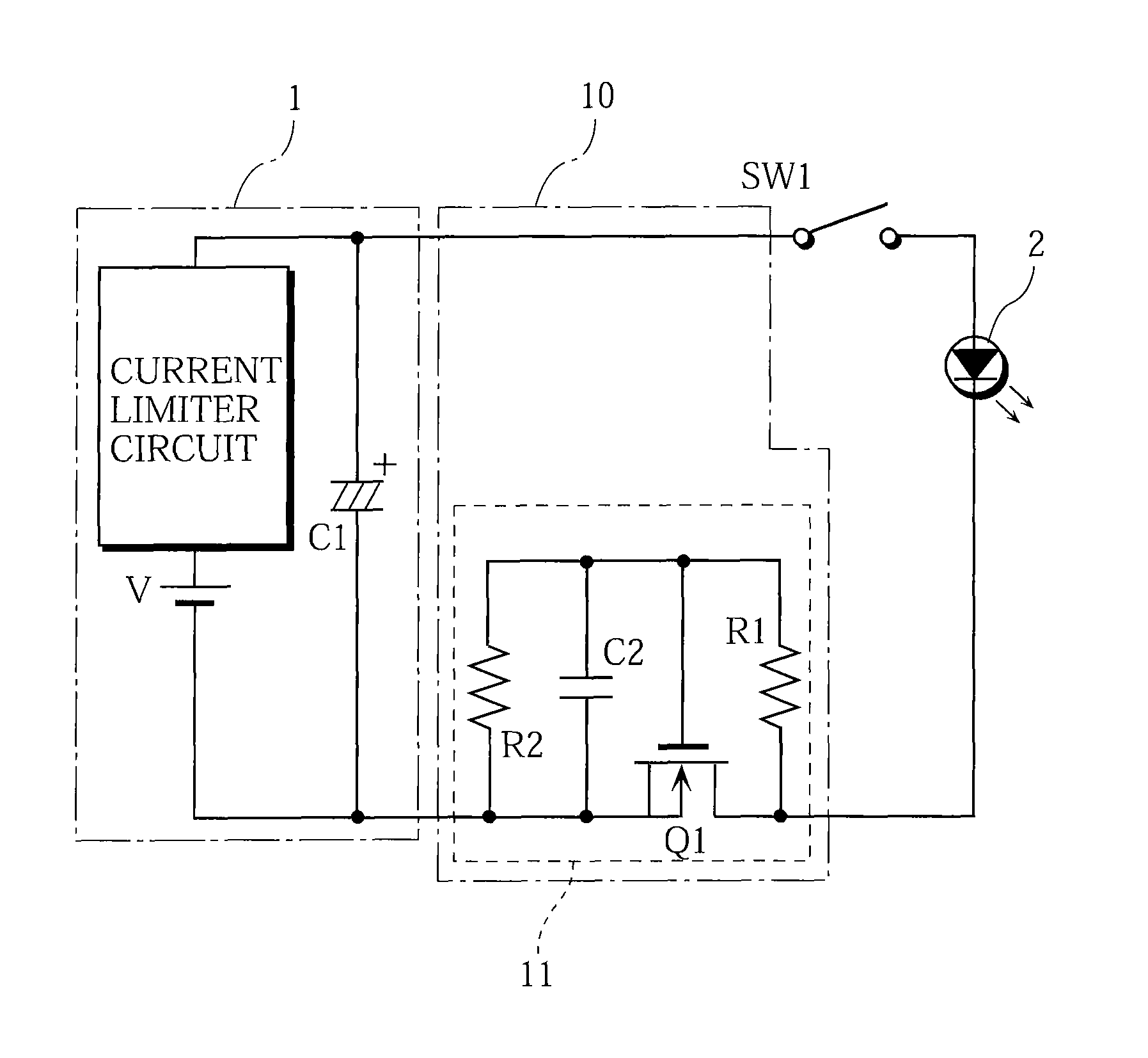
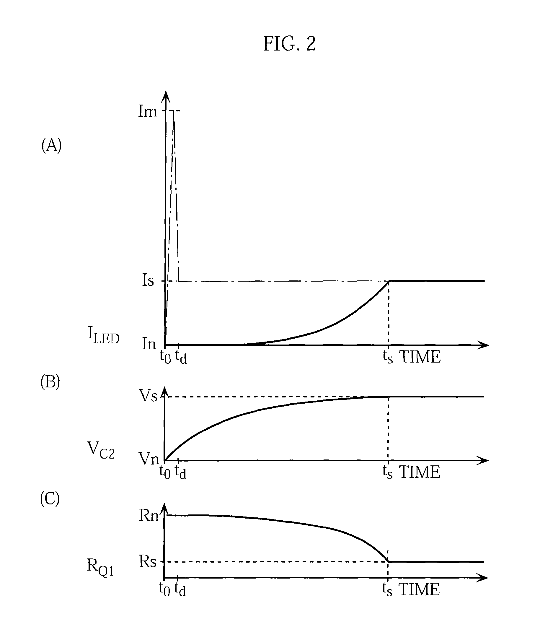
[0049]An element breakdown prevention circuit of Embodiment 1 will be described. FIG. 1 is a circuit diagram illustrating one example of the element breakdown prevention circuit according to Embodiment 1. FIG. 1 also shows a constant-current power supply 1 and an LED 2 along with the element breakdown prevention circuit 10. It should be noted that in FIG. 1, a switch SW1 is not a switch element that is provided separately from the LED 2 but is a virtual switch for representing a transition between the connected state and the disconnected state of the LED 2. An example is the case in which the electric circuit includes a first input / output terminal electrically connected to an output terminal (an upper wiring terminal) of the constant-current power supply 1, a second input / output terminal, an LED 2, and a socket (not shown) to which the LED 2 is detachably fixed, and by mounting the LED 2 to the socket, the first input / output terminal and the second input / output terminal are electric...

embodiment 2

[0064]An element breakdown prevention circuit according to Embodiment 2 has a configuration that can reduce the load due to the element breakdown prevention circuit itself in the steady phase of the connected state, in comparison with the element breakdown prevention circuit 10 according to Embodiment 1. FIG. 3 is a circuit diagram illustrating one example of the element breakdown prevention circuit according to Embodiment 2. The element breakdown prevention circuit 20 of the present embodiment has the same configuration as that of the element breakdown prevention circuit 10 (see FIG. 1) in Embodiment 1 above, except that it contains a resistance eliminating circuit 22. In the following description, the same parts as those in Embodiment 1 are denoted by the same reference numerals, and are not elaborated upon further.

[0065]The element breakdown prevention circuit 20 further includes a resistance eliminating circuit 22 (one example of the impedance decrease accelerating circuit: one ...

embodiment 3

[0074]An element breakdown prevention circuit 40 according to Embodiment 3 has a configuration that can prevent an LED (functional element) from breakdown and deterioration when mounting or demounting the functional element even if the transition from the connected state to the disconnected state or vice versa takes place a plurality of times at a very short time interval when mounting or demounting the functional element. FIG. 5 is a circuit diagram illustrating one example of the element breakdown prevention circuit according to Embodiment 3. The element breakdown prevention circuit 40 of the present embodiment shown in FIG. 5 has the same configuration as that of the element breakdown prevention circuit 20 (see FIG. 3) in Embodiment 2 above, except that it contains a resistance increase accelerating circuit 43 (one example of the impedance increase accelerating circuit: one example of a portion of the “voltage-dependent type switching-control circuit”). In the following descripti...


PUM


Abstract

A functional element is prevented from breakdown and deterioration because of mounting and demounting of the functional element immediately after cut-off of driving power from a constant-current power supply or during supply of the driving power.An electric circuit is configured to electrically connect a constant-current power supply 1 having a capacitance between an output terminal and a reference potential terminal and a detachable functional element 2 to each other. The electric circuit has an element breakdown prevention circuit 10 having a first circuit terminal connected to an output terminal of the constant-current power supply 1 through the functional element 2, and a second circuit terminal connected to the reference potential terminal of the constant-current power supply 1 through the functional element 2. The element breakdown prevention circuit 10 increases an impedance between the circuit terminals to a disconnected state impedance in response to a transition from a connected state, in which the functional element 2 is mounted, to a disconnected state, in which the functional element 2 is removed. The element breakdown prevention circuit 10 decreases the impedance between the circuit terminals to a connected-state impedance in response to a connection state transition.

Description

TECHNICAL FIELD[0001]The present invention relates to an electric circuit for connecting to each other a constant-current power supply and a detachable functional element driven by electric power from the constant-current power supply, and more particularly to an electric circuit that prevents the functional element from breakdown due to mounting and demounting of the functional element.BACKGROUND ART[0002]A typical conventional light-emitting apparatus turns on an LED as in the following manners. A resistor and an LED are connected in series to a constant-voltage power supply so that the resistor can adjust the current passing through the LED. Alternatively, as illustrated in FIG. 12(A), a current limiter circuit is connected between a constant-voltage power supply 1 and an LED 2 in series so that the current limiter circuit can adjust the current passing through the LED. However, when a resistor or a current limiter circuit is connected in series, the inserted resistor or current ...

Claims


Application Information

Patent Timeline
Patent Type & Authority Patents(United States)
IPC IPC(8): H02H9/08H01L33/00
CPCH05B33/0812H05B33/0845Y02B20/345H05B45/395H05B45/10H05B45/50Y02B20/30
Inventor YAMANO, HITOSHIHINAMOTO, SUMIAKI
Owner IDEC CORPORATION
Why Eureka
Try Eureka