Thin film memory device having a variable resistance

A resistive film and thin-film storage technology, applied in the fields of storage circuits, semiconductor integrated circuits, and storage devices, can solve problems such as characteristic destruction, and no specific disclosure of the structure and characteristics of the memory.

Inactive Publication Date: 2011-09-21
PANASONIC CORP
View PDF1 Cites 0 Cited by
  • Summary
  • Abstract
  • Description
  • Claims
  • Application Information

AI Technical Summary

Problems solved by technology

[0004] Although these materials are believed to have variable resistance, there is no specific disclosure of the structures and properties that these and other materials may be most suitable for memory
Moreover, the properties of these materials are destroyed in semiconductor processing

Method used


Image

  • Thin film memory device having a variable resistance
  • Thin film memory device having a variable resistance
  • Thin film memory device having a variable resistance

Examples


no. 1 example

[0048]

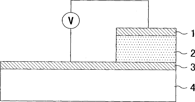
[0049] figure 1 The structure of the memory device according to the first embodiment of the present invention is shown. The memory device includes a lower electrode 3 formed on the surface of a substrate 4 , a variable resistance thin film 2 formed on the surface of the lower electrode 3 , and an upper electrode 1 formed on the variable resistance thin film 2 . The memory device can store information according to the resistance state of the variable resistance thin film 2 .

[0050] The resistance of the variable resistance thin film 2 can be changed according to the electric pulse applied thereto via the upper electrode 1 and / or the lower electrode 3. The upper electrode 1 and the lower electrode 3 can be formed of materials with low work function, such as Pt, Ru, Ir, Ag, Au, RuO 2 , or IrO 2 . It is necessary to use a material stable at the heating temperature for the lower electrode 3 because the variable resistance thin film 2 is usually formed by heating the ...

no. 2 example

[0143]

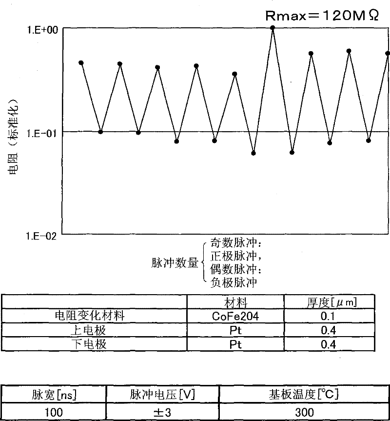
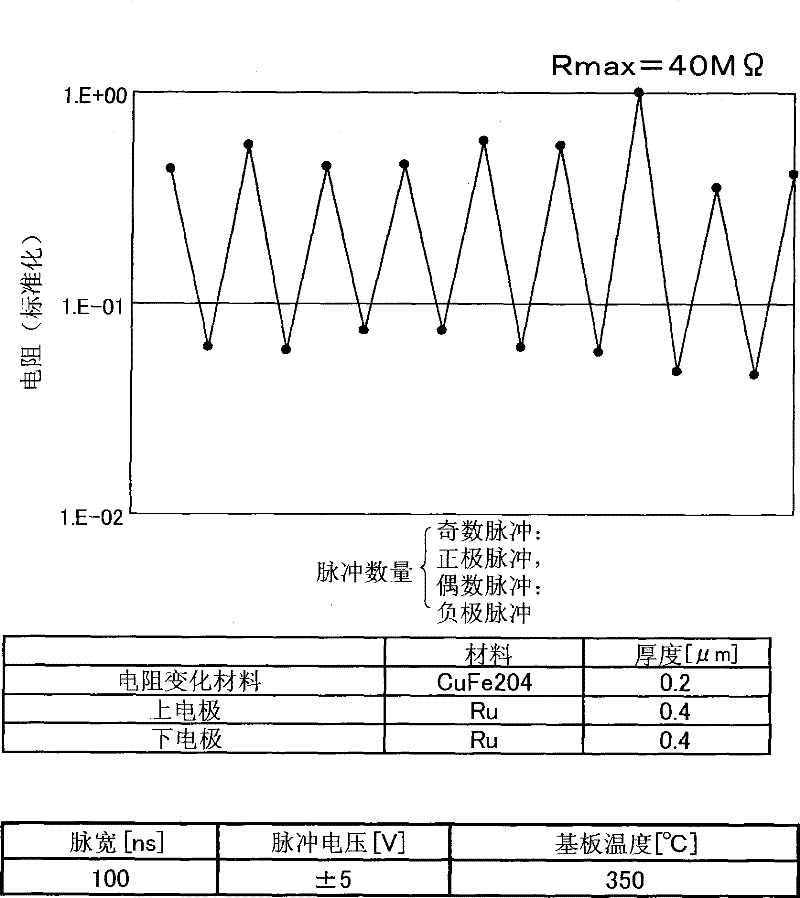
[0144] figure 1 The circuit labeling of the memory device shown is as Figure 9 Defined as shown in (a). memory device 101 is figure 1 shown in the memory device, figure 1 One of the shown upper electrode 1 and lower electrode 3 is connected to terminal 102 , and the other electrode is connected to terminal 103 . If an electrical pulse (voltage +E1) is applied that causes terminal 102 to have a positive polarity with respect to terminal 103, then as Figure 9 The resistance of the memory device 101 is reduced as shown in (b). Conversely, if an electrical pulse (voltage -E1) is applied that causes terminal 102 to have a negative polarity with respect to terminal 103, then as Figure 9 The resistance of the memory device 101 is increased as shown in (b). That is, if an electrical pulse is applied such that the current at Figure 9 The flow in the direction of the arrow in the memory device 101 shown in (a) reduces the resistance of the memory device 101 . If a...

no. 3 example

[0187]

[0188] Figure 13 (a) shows the structure of a memory cell used in a memory circuit according to a third embodiment of the present invention. This memory cell comprises two memory devices 101a and 101b between terminals 104a and 104b. The memory device 101 a has the same structure as the memory device 101 and is disposed between the terminals 104 a and 105 . The memory device 101b has the same structure as the memory device 101, and is disposed between the terminals 105 and 104b. The resistance of each memory device 101a and 101b is initialized. The resistance of the memory device 101a is a resistance Rb, and the resistance of the memory device 101b is a resistance Ra (Ra Figure 13 As shown in (a), if the potentials of the terminals 104a and 104b drop to the ground potential and an electric pulse (a positive pulse with a voltage of +E1) is applied to the terminal 105, then, as Figure 13 As shown in (b), the resistance of the memory device 101a decreases from the...


PUM


Abstract

A thin film storage device includes a first electrode (3), a first variable resistance thin film (2), and a second electrode (1). The first electrode (3) is formed over a surface of a substrate (4). The first variable resistance thin film (2) is formed over a surface of the first electrode (3). The second electrode (1) is formed over a surface of the first variable resistance thin film (2). The first variable resistance thin film (2) comprises a material whose resistance in a bulk state changes in accordance with at least one of a lattice strain and a change of charge-order.

Description

technical field [0001] The present invention relates to a memory device, a memory circuit and a semiconductor integrated circuit each having a variable resistance thin film. Background technique [0002] With the development of digital technology for electronic equipment, there is a strong demand for increasing the capacity of solid-state memory devices and accelerating data transfer in order to reduce the time for storing data. US Pat. No. 6,204,139 discloses a technique to meet these needs. This technique involves the use of perovskite materials (e.g., Pr 1-x Ca x MnO 3 (PCMO), LaSrMnO 3 (LSMO), or GdBaCo x o y (GBCO)) form a solid-state memory device, the perovskite material has a resistance that changes in response to an applied electrical pulse. Therefore, perovskite materials can be used to store different digital values. [0003] In addition, J.Appl.Phys., Vol.84(1998), p. 5647 proposes a memory element with deep main level and shallow donor level using an amo...

Claims


Application Information

Patent Timeline
Patent Type & Authority Patents(China)
IPC IPC(8): G11C11/34G11C16/02H01L45/00
CPCH01L45/147G11C2213/78G11C2213/79G11C2213/31G11C13/0007H01L45/146H01L45/145H01L45/04H01L45/1233G11C13/003Y10T428/1136Y10T428/115H10N70/20H10N70/8836H10N70/8833H10N70/826G11C11/14
Inventor 小佐野浩一村冈俊作榊间博
Owner PANASONIC CORP
Why Eureka
Try Eureka