Method for producing electric circuit device

A technology of circuit device and manufacturing method, applied in the direction of printed circuit manufacturing, circuit, printed circuit, etc., can solve the problems of lack of flatness, inability to use metal mold molding, etc.

Inactive Publication Date: 2002-05-08
SANYO ELECTRIC CO LTD
View PDF0 Cites 16 Cited by
  • Summary
  • Abstract
  • Description
  • Claims
  • Application Information

AI Technical Summary

Problems solved by technology

Thereafter, up to the covering resin layer of the above-mentioned production method, with Figure 22 The manufacturing method is the same, but the ceramic substrate is very brittle, and unlike flexible sheets or glass epoxy substrates, there is a problem that molding using a metal mold cannot be performed due to lack of flatness

Method used


Image

  • Method for producing electric circuit device
  • Method for producing electric circuit device
  • Method for producing electric circuit device

Examples


no. 1 Embodiment

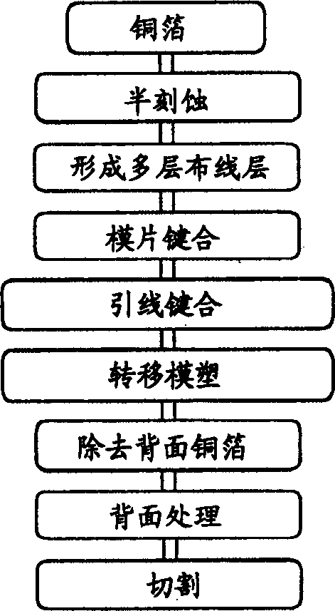
[0052] First, while referring to figure 1 , while explaining the manufacturing method of the circuit device of the present invention.

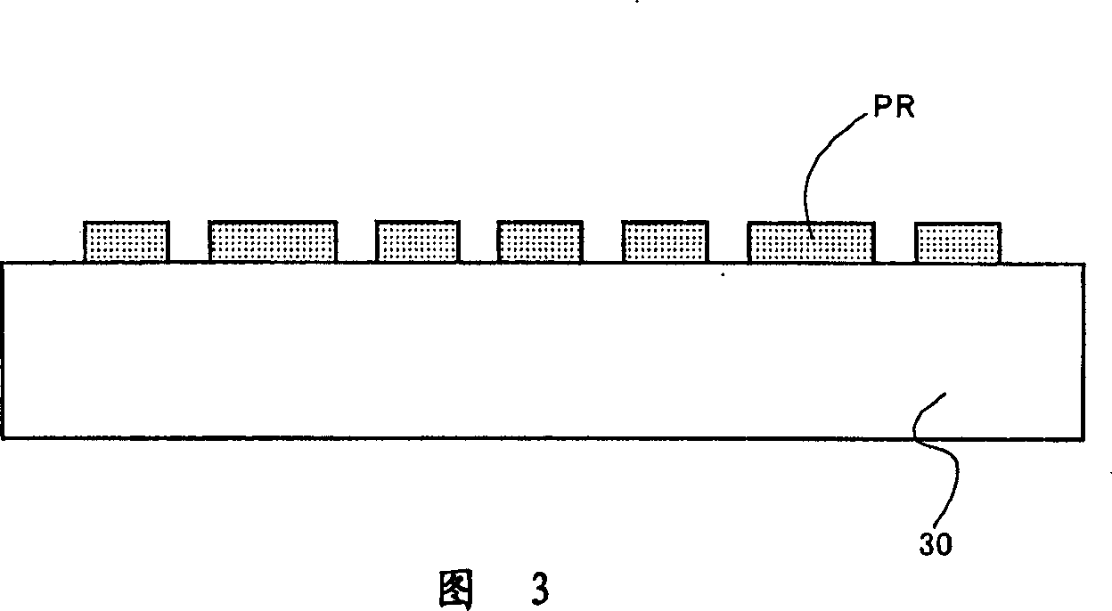
[0053] The present invention consists of the following steps: preparing a conductive foil, forming a separation groove shallower than the thickness of the conductive foil on the above-mentioned conductive foil in a region other than the first-layer conductive pattern to form a first-layer conductive pattern; The process of forming a multilayer conductive pattern through an interlayer insulating film on the first layer of conductive pattern; the process of assembling circuit components on the desired conductive pattern; covering the above circuit components with insulating resin and molding the whole Steps; a step of removing the conductive foil in the thickness portion where the separation groove is not provided; and a step of separating the insulating resin into the individual circuit elements by dicing.

[0054] figure 1 The flow shown i...

no. 2 Embodiment

[0091] First, while referring to Figure 11 , while explaining the manufacturing method of the circuit device of the present invention.

[0092] The present invention consists of the following steps: a step of preparing a conductive foil and forming a multilayer conductive pattern through an interlayer insulating film; a step of assembling a circuit element on the desired conductive pattern; covering the above-mentioned circuit element with an insulating resin, a step of molding the whole; a step of removing the conductive foil; and a step of separating the insulating resin into individual circuit devices including the respective circuit elements by dicing.

[0093] Figure 11 The flow shown in is different from the above-mentioned steps, but the conductive foil supporting the multilayer wiring layer formed thereon is prepared in two flows of Cu foil and Ag plating. A multilayer conductive pattern is formed on the conductive foil in the process of forming the multilayer wiri...


PUM


Abstract

A conductive pattern of a first layer isolated by an isolation trench is formed on a conductive foil, and a plurality of layers of the conductive patterns are formed thereon to create a multilayered wiring structure, and furthermore, a circuit element is mounted and molded with an insulating resin and the back surface of the conductive foil is etched. It is possible to implement a method of manufacturing a circuit device which provides very power saving and is suitable for mass production, then the circuit device having conductive patterns of a multilayered structure are provided.

Description

technical field [0001] The present invention relates to a method of manufacturing a circuit device, and more particularly to a method of manufacturing a circuit device that does not require multilayer wiring on a support substrate. Background technique [0002] Conventionally, since circuit devices mounted in electronic devices are used in mobile phones, portable computers, and the like, miniaturization, thinning, and weight reduction are required. [0003] For example, if a semiconductor device is described as an example of a circuit device, as a general semiconductor device, there has conventionally been a packaged semiconductor device sealed by normal transfer molding. The semiconductor device such as Figure 20 As shown, it is mounted on the printed substrate PS. [0004] In addition, in this packaged semiconductor device, the periphery of the semiconductor chip 2 is covered with the resin layer 3 , and the lead terminals 4 for external connection are led out from the s...

Claims


Application Information

Patent Timeline
Patent Type & Authority Applications(China)
IPC IPC(8): H01L21/48H01L21/56H01L21/68H01L23/31H05K3/00H05K3/06H05K3/20
CPCH01L2924/19105H01L2221/68377H01L2924/01082H01L2221/68345H01L23/3121H01L2224/97H01L2924/12041H01L2224/16H01L2924/09701H01L21/568H01L2924/15311H01L2924/01029H05K3/0058H01L21/6835H01L2924/19041H01L2224/48091H01L2224/48464H01L2924/01013H01L2924/01024H01L24/97H05K3/06H01L2924/19043H01L2924/01047H01L2924/01079H01L2224/48227H01L2924/14H01L2924/01005H01L2924/01033H01L2924/01006H01L2924/01059H01L2924/01078H01L21/4857H01L2224/73265H01L2224/85001H01L21/561H05K3/20H01L2224/05568H01L2224/05573H01L2924/00014H01L2924/12042H01L2924/13055H01L2924/15787H01L2924/181H01L2224/85H01L2224/83H01L2924/00H01L2224/05599H01L2924/00012
Inventor 坂本则明小林义幸阪本纯次冈田幸夫五十岚优助前原荣寿高桥幸嗣
Owner SANYO ELECTRIC CO LTD
Why Eureka
Try Eureka