Deformation-resistant installation structure for portable apparatus

A technology for portable devices and installation structures, which is applied in the direction of support structure installation, printed circuit stress/deformation reduction, electrical equipment structural parts, etc., and can solve the problem of reduced effective area of ​​printed circuit boards and insufficient absorption of external mechanical stress And other issues

Inactive Publication Date: 2002-07-17
NEC CORP
View PDF2 Cites 8 Cited by
  • Summary
  • Abstract
  • Description
  • Claims
  • Application Information

AI Technical Summary

Problems solved by technology

[0011] Specifically, only a set of long hole shapes or grooves formed around the portion for fixing the printed wiring board to the case cannot prevent the deformation of the printed wiring board, nor can the mechanical stress of the external force be sufficiently absorbed, Also, the effective area of ​​the printed wiring board will be reduced due to the portion formed with a long hole shape or a long groove

Method used


Image

  • Deformation-resistant installation structure for portable apparatus
  • Deformation-resistant installation structure for portable apparatus
  • Deformation-resistant installation structure for portable apparatus

Examples


no. 1 example

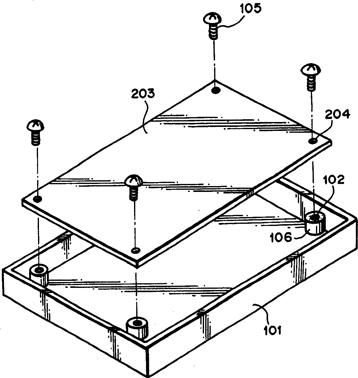
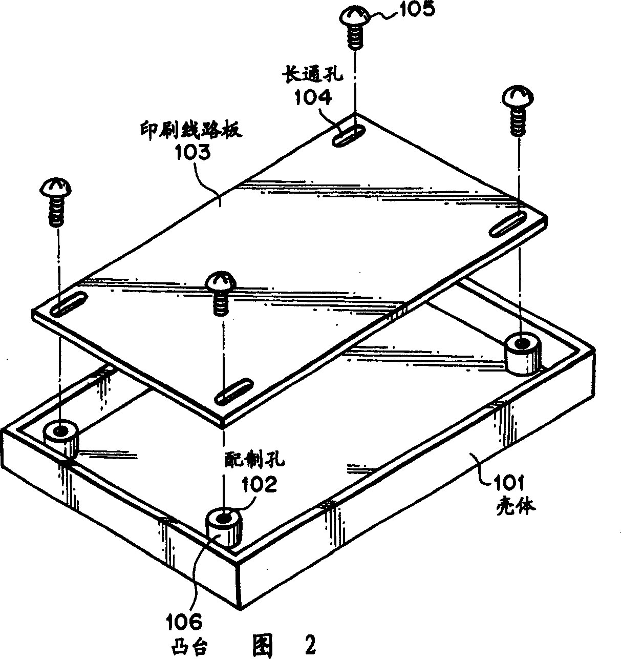
[0035] Refer to Figure 2 to Figure 4 , the boss 106 formed with the preparation hole 102 is disposed at the corner of the housing 101 . The preparation hole 102 is suitable for tap tapping. The preparation holes can also be replaced by threaded holes.

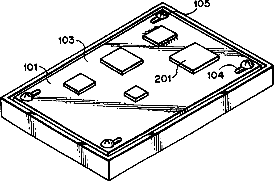
[0036] In order to reduce external mechanical stress applied to the printed wiring board 103 , the holes passed by the screws 105 are long through holes 104 formed on the printed wiring board 103 .

[0037] Specifically, as described above, in the printed wiring board 103, the long through hole 104 is formed at a position corresponding to the boss 106 on the housing 101, as shown in Fig. 2 and Figure 4 shown. In the example of the first embodiment, the long through holes 104 are formed in the longitudinal direction at the four corners of the printed wiring board 103 . However, the long through hole 104 may also be formed in a direction perpendicular to the longitudinal direction or in any direction.

[0038] The printed ...

no. 2 example

[0040] exist Figure 5A and 5BIn the second embodiment of the present invention, in order to further reduce the external mechanical stress applied to the printed circuit board 103, a through boss 401 is used, and the through boss 401 includes a central part 402, the central part 402 is formed as a part with a smaller diameter through the long through hole 104 on the printed circuit board 103, and the central part 402 has a preparation hole 102, the through boss 401 also includes a part 404 with a larger diameter, This part has a base 403 for mounting the printed wiring board 103, although usually the printed wiring board 103 is fixed between the bosses 106 with the prepared holes 102 and the screws 105. It is desirable to make the inner diameter of the long through hole 104 slightly larger than the outer diameter of the central portion 402 so that the central portion 402 can freely displace in the long through hole 104 .

[0041] In addition, in order to smoothly displace th...


PUM


Abstract

Disclosed is a novel deformation-resistant structure of a portable device, capable of reducing an electric failure by decreasing a distortion which occurs in a soldered portion between a printed circuit board of the portable device and an electric part mounted on the board due to a mechanical stress such as drop or pressure. Through slits are formed in positions in a printed wiring plate, which correspond to bosses having prepared holes disposed at the corners of a casing. By inserting screws into the prepared holes through the through slits, the printed circuit board is mounted in the casing. Although the casing is deformed when an external mechanical stress is applied to the casing, the screw and the boss can slide along each of the through slits. Thus, a deformation amount of the printed circuit board is not caused or becomes smaller than that of the casing.

Description

technical field [0001] The present invention relates to a printed circuit board of a portable device such as a portable phone, PHS or PDA and a casing structure in which the printed circuit board is installed, in particular to a deformation-proof installation structure of the portable device. Background technique [0002] As portable devices such as portable phones or PDAs become lighter, thinner, and smaller, a user can conveniently carry them in his / her pocket or the like. [0003] Fig. 1 is an exploded perspective view showing a general schematic structure of this prior art. [0004] In FIG. 1, a set of screws 105 are inserted into the through holes 204 of the printed circuit board 203, and screwed into the preparation holes 102 on the boss 106 of the housing 101, thereby clamping the printed circuit board 203 of the portable device to the boss. Between the top surface of 106 and the screw 105 , the printed wiring board 203 is mounted on the housing 101 . [0005] Since...

Claims


Application Information

Patent Timeline
Patent Type & Authority Applications(China)
IPC IPC(8): H05K5/00H05K1/02H05K7/14
CPCH05K2201/09854H05K2201/10409H05K2201/09063H05K7/142H05K2201/10598H05K1/0271
Inventor 水崎学
Owner NEC CORP
Why Eureka
Try Eureka