Formation of pulse signal from clock signal

A pulse signal and clock signal technology, applied in pulse processing, pulse technology, delay line pulse generation, etc., can solve problems such as reducing the clock signal cycle

Inactive Publication Date: 2002-07-24
SEIKO EPSON CORP
View PDF0 Cites 5 Cited by
  • Summary
  • Abstract
  • Description
  • Claims
  • Application Information

AI Technical Summary

Problems solved by technology

[0014] In this way, in the conventional pulse signal generation circuit, in order to satisfy the required value for a specific period of the pulse signal, there is a problem that the cycle of the clock signal must be greatly reduced in consideration of the fluctuation of the delay time in the delay element.

Method used


Image

  • Formation of pulse signal from clock signal
  • Formation of pulse signal from clock signal
  • Formation of pulse signal from clock signal

Examples


Embodiment approach

[0039] A. The first embodiment;

no. 2 Embodiment ;

[0041] C. The third embodiment;

[0042] D. The fourth embodiment;

[0043] E. The fifth embodiment;

[0044] F. The sixth embodiment;

[0045] G.Modification

no. 1 Embodiment

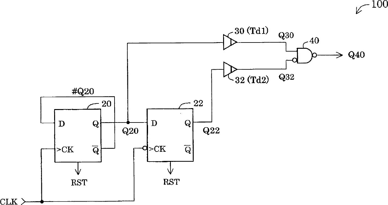
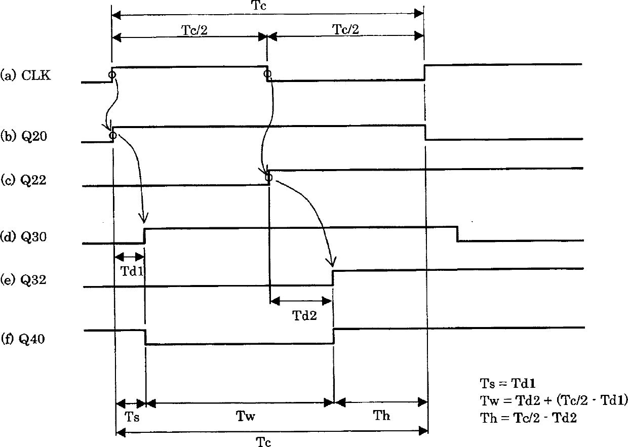
[0047] figure 1 It is a block diagram showing the configuration of the pulse signal generating circuit 100 as the first embodiment of the present invention. This pulse signal generating circuit 100 includes two D flip-flops 20, 22, two delay elements 30, 32, and a NAND gate 40 in which one of the two input terminals is a non-inverting input terminal. In addition, hereinafter, the "D flip-flop" is referred to as "DFF".

[0048] The clock signal CLK is input to the clock input terminal of the first DFF 20 and input to the clock terminal of the second DFF 22 after being inverted. The inverted output #Q20 of the first DFF20 is fed back to the D input terminal of the first DFF20. The output Q20 of the first DFF 20 is input to the D input terminal of the second DFF 22 and also input to the first delay element 30 . The output Q22 of the second DFF 20 is input to the second delay element 32 . The first delay signal Q30 delayed by the first delay element 30 is input to the non-inv...


PUM


Abstract

Providing technology capable of satisfying a request value concerning the specified period of a pulse signal, without excessively lowering the cycle of a clock signal, even if considering fluctuation in delay time is taken into consideration, in a delay element. Two first delay signals Q30 and Q34 are generated such that edges thereof are delayed by a first delay time Td1 in relation to the rising edge of a clock signal CLK. Two second delay signals Q32 and Q36 are also generated such that edges thereof are delayed by a second delay time Td2 in relation to the trailing edge of the clock signal CLK. A pulse signal Sout is generated as a result of logic operations performed on the first delay signals Q30 and Q34 and the second delayed signals Q32 and Q36.

Description

technical field [0001] The present invention relates to a technique for generating a specific pulse signal from a clock signal of a certain period. Background technique [0002] Figure 13 It is a block diagram showing an example of a conventional pulse signal generating circuit 200 for generating a specific pulse signal Q230 from a clock signal CLK. This circuit 200 includes a D flip-flop 210 (hereinafter referred to as "DFF 210"), two delay elements 220 and 222 connected in series, and a NAND gate 230 with one of the two input terminals serving as an inverting input terminal. A clock signal CLK is supplied to a clock input terminal of DFF 210 . The output Q210 of the DFF 210 is input to the first delay element 220, and the inverted output #Q210 is fed back to the D input terminal. The delay signal Q220 delayed by the first delay element 220 is input to the non-inverting input terminal of the NAND gate 230 . In addition, the delayed signal Q220 is input to the inverting ...

Claims


Application Information

Patent Timeline
Patent Type & Authority Applications(China)
IPC IPC(8): H03K5/135G06F1/12H03K3/86H03K5/13H03K5/14H03L7/00
CPCH03K5/135H03K5/131
Inventor 大塚修司
Owner SEIKO EPSON CORP
Why Eureka
Try Eureka