Buffer amplifier architecture for semiconductor memory circuits

a buffer amplifier and memory circuit technology, applied in the direction of information storage, static storage, digital storage, etc., can solve the problems of undesirable inability to change the clock delay, the delay time range of registers and buffer amplifier architectures used in conventional semiconductor memory modules provided with registers is often too high,

Active Publication Date: 2005-05-17
POLARIS INNOVATIONS
View PDF4 Cites 81 Cited by
  • Summary
  • Abstract
  • Description
  • Claims
  • Application Information

AI Technical Summary

Benefits of technology

[0005]An exemplary embodiment of the present invention provides an architecture, applicable to buffer amplifiers and registers, that contains an adjustable delay and a fixed-delay feedback loop, which electrically encompasses the same path as the usual command ...

Problems solved by technology

In this context, the delay time range of registers and buffer amplifier architectures that are used in conventional semiconductor memory modules provided with registers is frequently too high.
The setting ...

Method used


Image

  • Buffer amplifier architecture for semiconductor memory circuits
  • Buffer amplifier architecture for semiconductor memory circuits
  • Buffer amplifier architecture for semiconductor memory circuits

Examples


Embodiment Construction

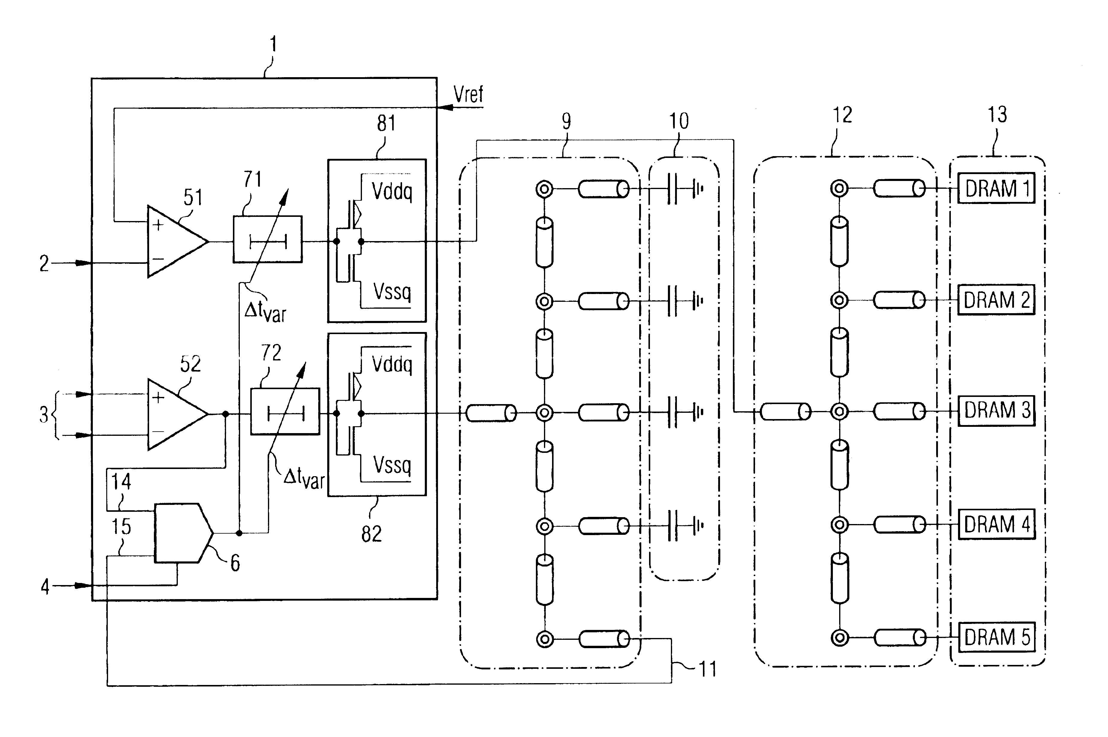
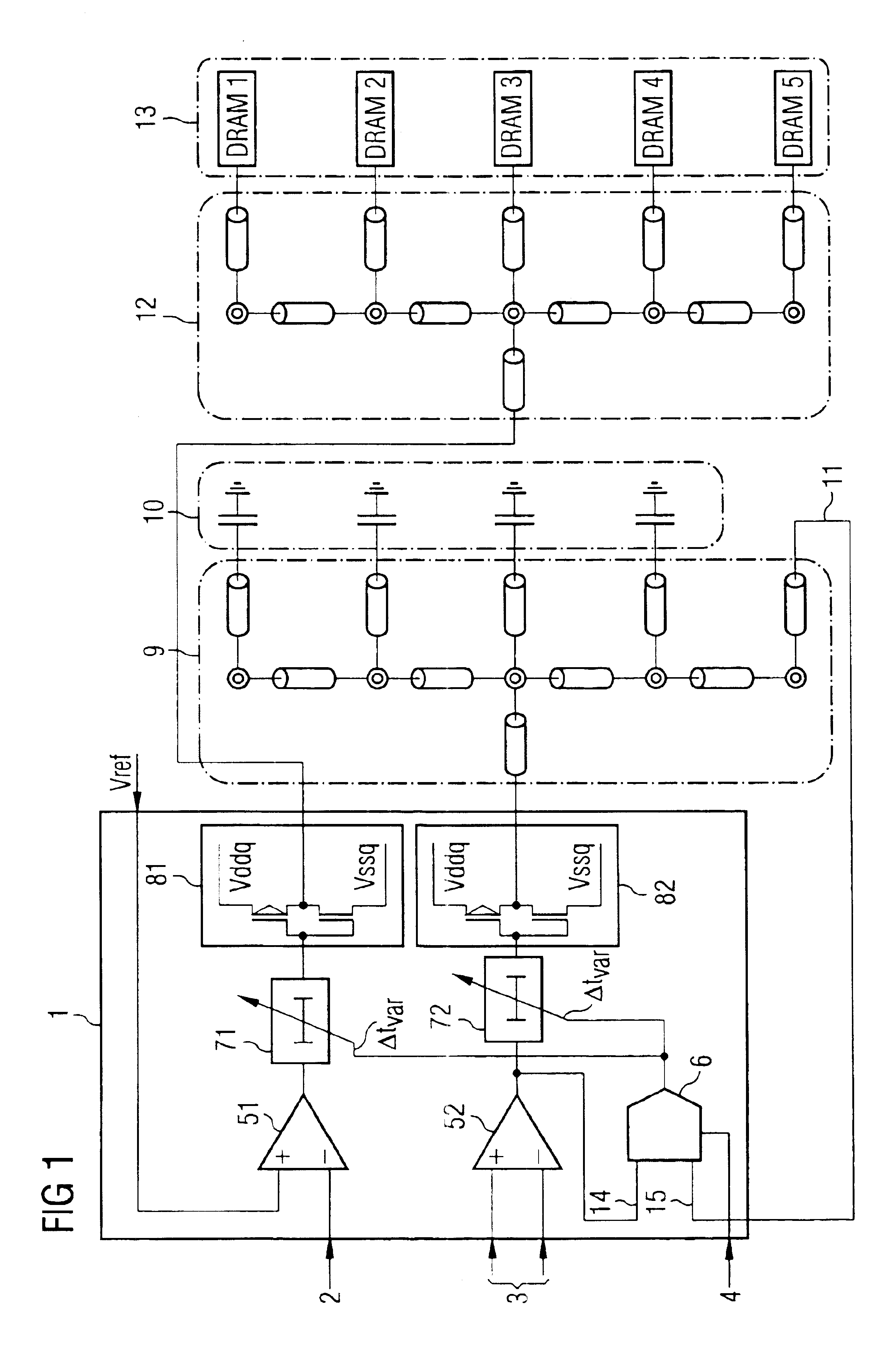
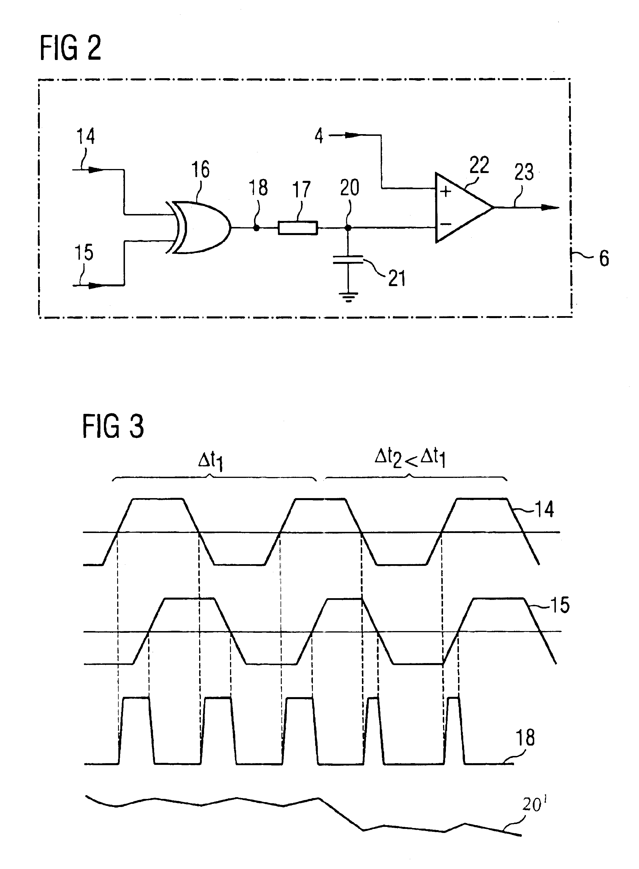
[0015]The following list of symbols is used consistently throughout the text and drawings.[0016]1 Buffer amplifier architecture[0017]2 Command-address signals[0018]3 Clock signal[0019]4 Reference signal[0020]51, 52 First and second receiver elements[0021]6 Delay detector circuit[0022]71, 72 First, second delay circuits[0023]81, 82 First, second output buffer amplifiers[0024]9 Reference line network[0025]10 Terminating capacitance elements[0026]11 Feedback loop[0027]12 Signal line network[0028]13 DRAM memory chips[0029]14, 15 First and second input for the delay detector circuit 6[0030]16 Exclusive-OR gate[0031]17 Resistor[0032]18 Output of the exclusive-OR gate[0033]20 Output of an integration circuit[0034]21 Capacitor[0035]22 Differential amplifier[0036]23 Output of the differential amplifier 22[0037]80 Register

[0038]Referring to FIG. 1, a buffer amplifier architecture, denoted generally by 1, contains a first receiver element 51, in the form of a differential amplifier for receivi...


PUM


Abstract

A buffer amplifier architecture for buffering signals which are supplied in parallel to identical chips, particularly DRAM chips, on a semiconductor memory module, is disclosed. The architecture has adjustable delay circuits in each signal line and a delay detector circuit which receives a clock signal from the buffer amplifier architecture at the input and at the output of the buffer amplifier architecture, and takes the phase difference between the two signals to produce a control signal for setting the variable delay time of the delay circuits. To ensure that the delay time set by the delay detector circuit is independent of variations in parameters of the DRAM memory chips, the feedback path routed to the input of the delay detector circuit has a reference line network of the same structure and having the same electrical properties as capacitance elements which terminate the line network routed to the DRAM memory chips and the reference line network, and which have the same capacitances as the signal inputs on the DRAM memory chips.

Description

BACKGROUND[0001]1. Field of the Invention[0002]The present invention relates to design of semiconductor memory circuits. More particularly, it relates to a buffer amplifier architecture for buffering signals that are supplied in parallel to identical chips on a semiconductor circuit module, particularly DRAM chips on a DRAM memory module.[0003]2. Background Information[0004]In semiconductor memory modules, for example DRAM memory modules, which are clocked at ever higher frequencies, it is paramount that signals supplied to a group of identical chips in parallel, such as address, command and data signals, should have the same signal propagation time to the extent possible. In this context, the delay time range of registers and buffer amplifier architectures that are used in conventional semiconductor memory modules provided with registers is frequently too high. The delay time typically ranges from 0.9 ns to 2.5 ns. As a result, at frequencies above 100 mHz, the time tolerances of t...

Claims


Application Information

Patent Timeline
IPC IPC(8): G11C7/10G11C11/4093G11C11/409
CPCG11C7/1078G11C7/1084G11C11/4093G11C7/1093G11C7/109
Inventor KUZMENKA, MAKSIMKIEHL, OLIVER
Owner POLARIS INNOVATIONS
Why Eureka
Try Eureka