

Surface fitting device package lead connecting method
A wire bonding and wire bonding technology, applied in the field of new wire bonding, can solve problems such as misalignment, complicated manufacturing process, easy damage or cracking
- Summary
- Abstract
- Description
- Claims
- Application Information
AI Technical Summary
Problems solved by technology
Method used
Image

Examples
Embodiment Construction
[0029] A wire bonding method for an SMD package according to the present invention will be described in detail below.
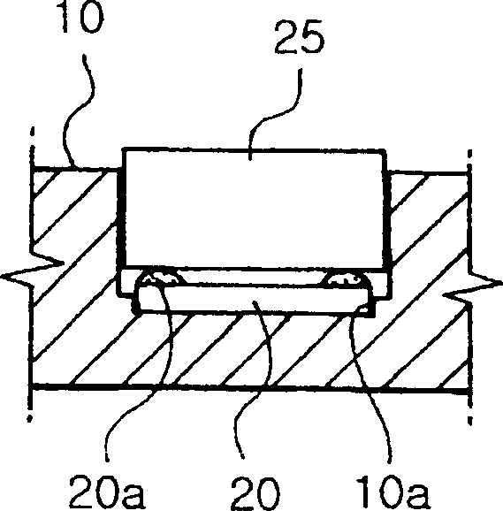
[0030] Figures 3a to 3d Schematic representation of the steps of a wire bonding method for an SMD package. First, if Figure 3a As shown in , the package 25 is arranged in the positioning groove of the support table 42 to allow the lead positioning surface of the package 25 on which the leads are positioned to face upward. The supporting platform 42 is made of common non-magnetic material or graphite material, and has a plurality of positioning grooves. Each positioning groove of the support platform 42 does not have to have the same size as the package or have a stepped structure like the positioning grooves of a conventional graphite jig. Therefore, the jig of the present invention can be easily manufactured and can prevent misalignment due to breakage of the stepped structure.
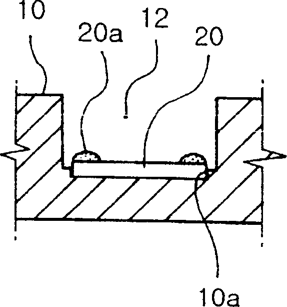
[0031] Such as Figure 3b As shown in , the leads 20 are positioned in t...
PUM
 Abstract
Description
Claims
Application Information