Method and system for detecting defects on a printed circuit board

A technology for printed circuit boards and defects, applied to printed circuits, printed circuit manufacturing, electrical components, etc., can solve problems such as difficulty in collecting quantitative information and slow speed

Inactive Publication Date: 2003-03-05
SOLVISION
View PDF2 Cites 37 Cited by
  • Summary
  • Abstract
  • Description
  • Claims
  • Application Information

AI Technical Summary

Problems solved by technology

Visual inspection has several drawbacks: subjectivity, slow speed, difficulty in gathering quantitative information on defects, etc.
This is a major disadvantage since faulty manufacturing processes can cause this recurring defect

Method used


Image

  • Method and system for detecting defects on a printed circuit board
  • Method and system for detecting defects on a printed circuit board
  • Method and system for detecting defects on a printed circuit board

Examples


Embodiment Construction

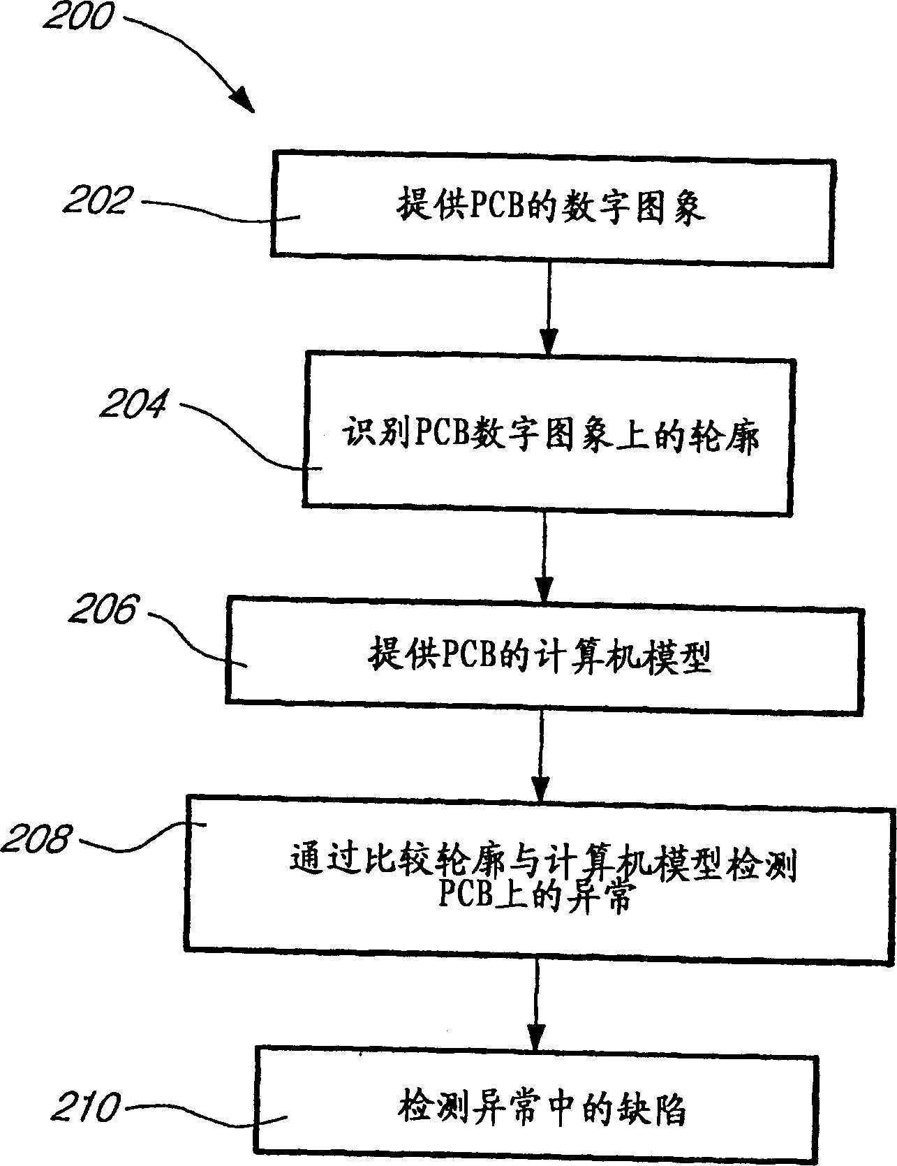
[0052] In general, a method for detecting PCB surface defects according to an embodiment of the present invention includes 1) identifying edges on a digital image of the PCB, 2) detecting anomalies by comparing the identified edges with a computer model of the PCB, and 3) detecting anomalies by The characterization of each anomaly determines whether the detected anomaly corresponds to a defect in the surface.

[0053] The method according to the invention thus proposes two levels of inspection: a first level, which allows rapid identification of anomalies and requires relatively little computation time, and a second level, which is a more refined inspection, comparing identified anomalies with design specifications, in order to characterize the detected defects.

[0054]To implement this method, a digital image of the inspected PCB and a computer model of a similar PCB must be provided.

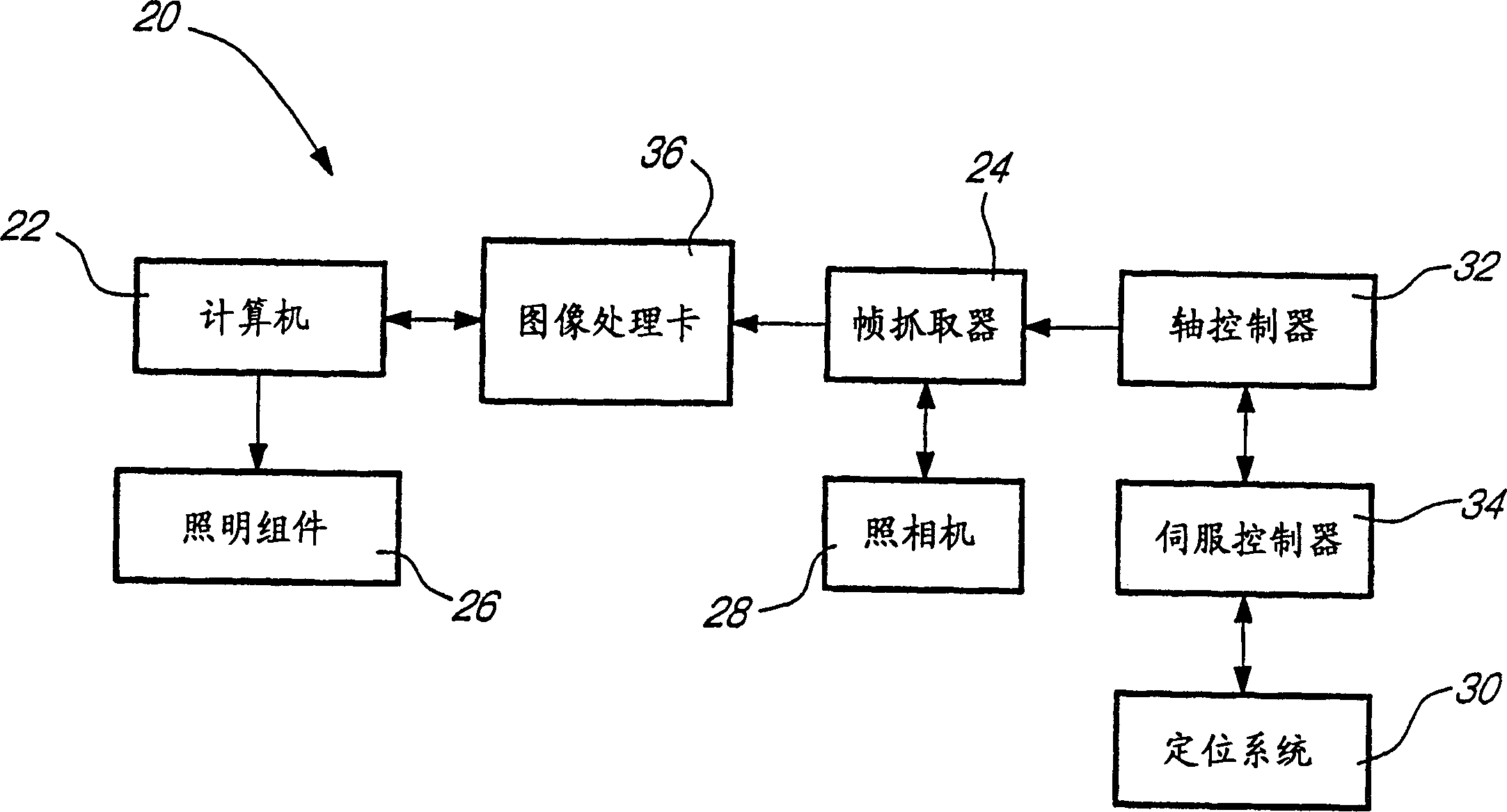
[0055] see attached figure 2 , a system 20 for detecting PCB surface defects according...


PUM


Abstract

A method and a system for detecting surface defects on electronic circuits, such as Printed Circuit Boards (PCB), are described herein. The method first comprises identifying contours on a digital image of the PCB. Then anomalies are detected on the PCB image by comparing the identified contours to contours on a vectorial model of the PCB. Each detected anomally is compared to manufacturing data to verify it if corresponds to a defect.

Description

technical field [0001] The present invention relates to inspection systems and methods for detecting defects on electronic circuits, such as printed circuit boards. More specifically, the present invention relates to edge detection based systems and methods. Background technique [0002] Electronic circuits can take many forms, such as PCBs (printed circuit boards), lead frames, hybrid circuits. These circuits usually contain multiple components (components) such as conductors, vias, solder joints, dielectrics, photopolymer protective films, and more. These components can be assembled in layers one on top of the other. An example of such a multilayer assembly is the well known conductor-hole-glaze circuit structure. In the following description, we will only refer to a printed circuit board (PCB) as an example. It should however be understood that the invention is not limited to this embodiment of an electronic circuit. [0003] In the past, inspection of PCBs was done ...

Claims


Application Information

Patent Timeline
Patent Type & Authority Applications(China)
IPC IPC(8): G01B11/30G01N21/956G06T1/00G06T7/60H05K3/00
CPCG06T2207/30141G06T7/0006H05K3/00
Inventor A·考奥贝M·坎廷L·贝拉尔J·戈泽尔
Owner SOLVISION
Why Eureka
Try Eureka