Mask-pattern correction method

A correction method and mask pattern technology, applied in the field of photolithography, can solve problems such as easy formation of depressions, and achieve the effects of improving uniformity, reducing writing and viewing time, and reducing file size

CN1405634AInactive Publication Date: 2003-03-26UNITED MICROELECTRONICS CORP
0 Cites 22 Cited by

Patent Information

Authority / Receiving Office
CN · China
Patent Type
Applications(China)
Current Assignee / Owner
Publication Date
2003-03-26
Estimated Expiration
Not applicable · inactive patent

Smart Images

  • Figure 1
    Figure 1
  • Figure 2
    Figure 2
  • Figure 3
    Figure 3
Patent Text Reader

Abstract

A correction method for mask patterns is first of all to provide a third pattern composed of a first strip pattern and a second pattern in which the first strip pattern is connected between the head and end of the second one, then two sides of the first strip pattern are added by an auxiliary pattern to form a first correction apttern. After that part of the first strip pattern is reduced to form a second correction pattern, the dimension of the reduced first strip pattern is the key on of a main pattern then the second correction pattern is modified by an optical adjacent correction method to form a third modified pattern.
Need to check novelty before this filing date? Find Prior Art

Description

Technical field

[0001] The present invention relates to a photolithography (Photolithography) process, and more particularly to a method for correcting mask patterns. Background technique

[0002] As the integration of integrated circuits increases, the component size of the entire integrated circuit must be reduced accordingly. The most important thing in the semiconductor process is the photolithography process, which is usually related to the structure of the Metal-Oxide-Semiconductor (MOS) device, such as the pattern of each layer of thin film (Pattern) and doped with impurities The area of ​​(Dopants) is determined by the step of photolithography. In order to reduce the size of components, some methods to improve the resolution of the mask have been continuously proposed, such as Optical Proximity Correction (OPC) and Phase Shift Mask (PSM) and so on.

[0003] The purpose of the optical proximity correction method is to eliminate the critical dimens...

Examples

Embodiment Construction

[0034] Figure 3A to Figure 3D As shown, it is a schematic flowchart of a method for correcting a mask pattern according to a preferred embodiment of the present invention.

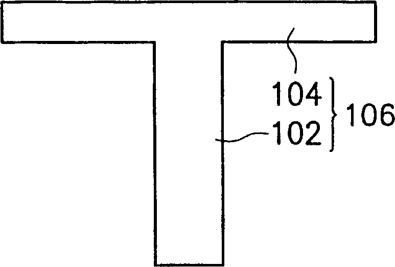
[0035] Please refer to Figure 3A First, a T-shaped original pattern 306 composed of a first long strip pattern 302 and a second long strip pattern 304 is provided. The first elongated original pattern 302 is connected to the middle section of the second elongated pattern 304.

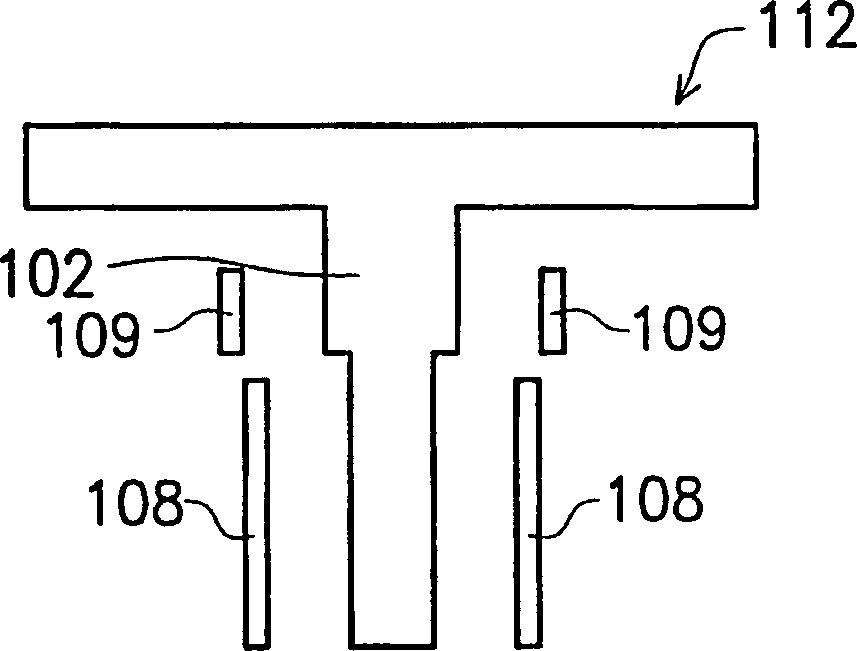
[0036] After that, please refer to Figure 3B , Perform a first correction step, add an auxiliary pattern 308 on both sides of the first strip pattern 302 to form a first correction pattern 310, wherein the first correction pattern 310 includes a T-shaped original pattern 306 and an auxiliary pattern 308. The shape of the auxiliary pattern 308 is, for example, a stripe shape.

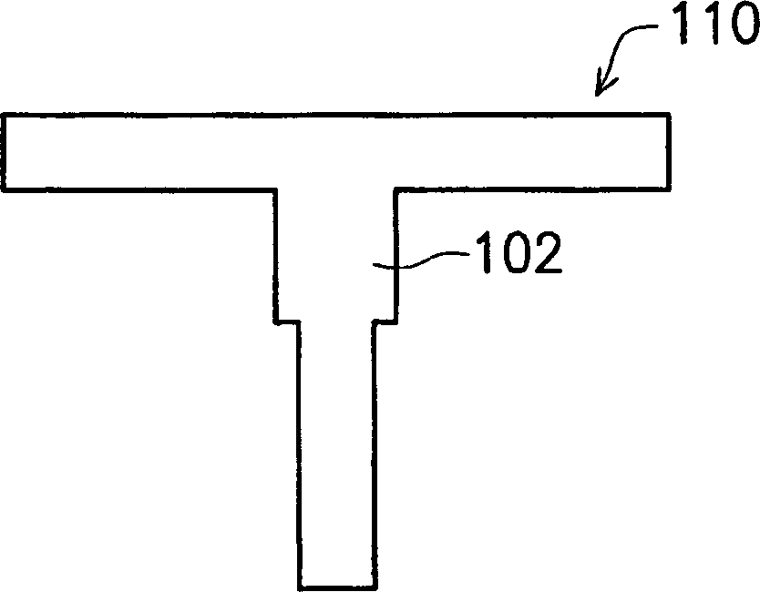
[0037] Next, please refer to Figure 3C , A second correction step is performed to reduce a portion of the first strip-shaped pattern 302 to form a second cor...