Ceramic electronic part, coating method and device

A technology of electronic components and ceramics, which is applied in the field of ceramic electronic components, slurry coating and slurry coating devices, and can solve the problems of ceramic substrate elevation and other issues

Inactive Publication Date: 2003-09-24
TDK CORPARATION
View PDF0 Cites 16 Cited by
  • Summary
  • Abstract
  • Description
  • Claims
  • Application Information

AI Technical Summary

Problems solved by technology

Therefore, the terminal electrodes are subjected to different stresses due to the solder and cause defects such as the ceramic substrate lifting phenomenon (Manhattan phenomenon)

Method used


Image

  • Ceramic electronic part, coating method and device
  • Ceramic electronic part, coating method and device
  • Ceramic electronic part, coating method and device

Examples


Embodiment Construction

[0037] Ceramic Electronic Components

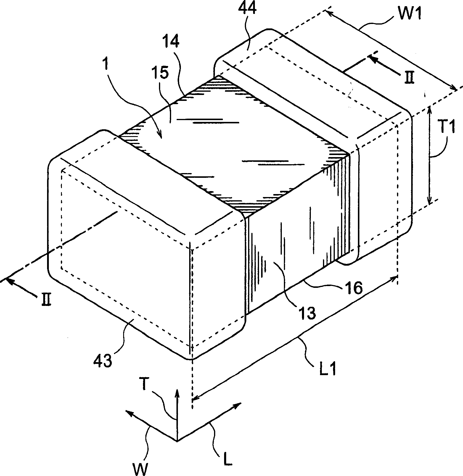
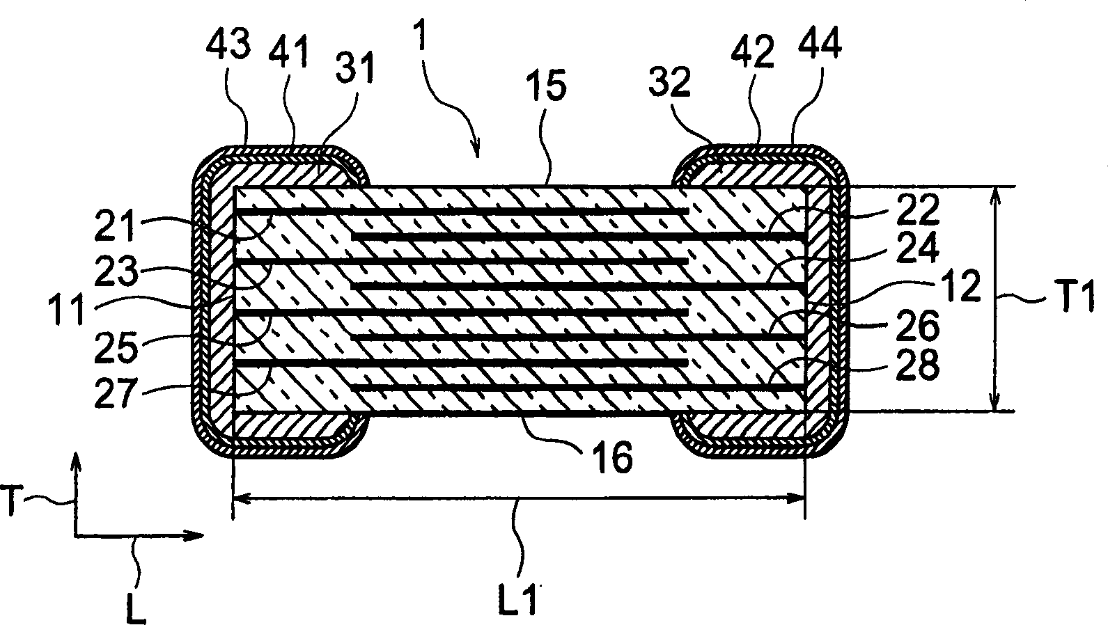
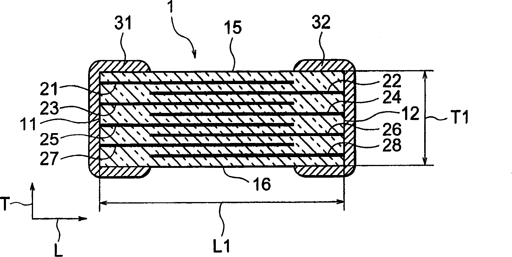
[0038] Such as figure 1 and figure 2 As shown, a ceramic electronic component according to one embodiment of the present invention has a ceramic base 1 and terminal electrodes 31 , 32 . Ceramic electronic components include chip capacitors, chip inductors, chip varistors or chip resistors or combinations thereof. In addition, a chip capacitor is shown as an example of a ceramic electronic component.

[0039] The ceramic base 1 is roughly in the shape of a cuboid. In addition, the substantially rectangular parallelepiped appearance also includes a rectangular parallelepiped whose corners are rounded or a rectangular parallelepiped with chamfered edges. The length L1 in the longitudinal direction L, the width W1 in the lateral direction W, and the thickness T1 in the thickness direction T in the ceramic base 1 are arbitrary. In the illustrated embodiment, length L1 = 2.0 mm, width W1 = 1.2 mm, and thickness T1 = 1.25 mm. Alternativ...


PUM

PropertyMeasurementUnit
lengthaaaaaaaaaa
thicknessaaaaaaaaaa
thicknessaaaaaaaaaa

Abstract

A ceramic capacitor having a ceramic body and terminal electrodes, the ceramic body being substantially a rectangular parallelopiped in shape, the terminal electrodes being provided at the two ends of the ceramic body in the length direction, each terminal electrode being provided to cover one end face of the ceramic body in the length direction, part of the two surfaces in the width direction, and part of the two surfaces in the thickness direction, wherein, when the length of the ceramic body is L1 and the maximum lengths of the terminal electrodes at the two surfaces of the ceramic body in the width direction are L3 and L4, 0<=|(L4-L3|/L1<=0.0227 is satisfied. One surface among the two surfaces of the ceramic body in the width direction is the paste introduction side in the roller coating, while the other surface is the paste escape side in the roller coating.

Description

technical field [0001] The present invention relates to a ceramic electronic component, a paste coating method and a paste coating apparatus used in the manufacture of the ceramic electronic component. Background technique [0002] In ceramic electronic components such as chip capacitors, cap-shaped terminal electrodes are formed on both longitudinal ends of a ceramic substrate. In detail, each cap-shaped terminal electrode is configured to cover one end surface of the ceramic base in the longitudinal direction, a part of both sides of the ceramic base in the transverse direction, and a part of both sides of the ceramic base in the thickness direction. [0003] To form such terminal electrodes, a method of immersing the ceramic substrate in the conductive paste or a roll coating method is used, that is, the conductive paste is generally coated on both ends of the ceramic substrate and dried and solidified by heat treatment. [0004] In the terminal electrodes formed by the ...

Claims


Application Information

Patent Timeline
Patent Type & Authority Applications(China)
IPC IPC(8): H01G4/252H01G2/06H01G4/232H01G4/30H01G13/00H05K3/34
CPCB05B1/08B05C1/027B05C11/025H01C1/148H01C17/281H01G2/065H01G4/232H01G13/006H05K3/3442H05K2201/09381H05K2201/10636Y02P70/50Y10T29/435
Inventor 横山英树武田笃史
Owner TDK CORPARATION
Why Eureka
Try Eureka