Schottky shielding dioe with low straightforward voltage drop and its producing method

A manufacturing method and forward voltage technology, applied in semiconductor/solid-state device manufacturing, circuits, electrical components, etc., can solve problems such as the inability to provide low forward voltage drop

Inactive Publication Date: 2003-10-01
ONIZUKA ELECTRONICS
View PDF0 Cites 5 Cited by
  • Summary
  • Abstract
  • Description
  • Claims
  • Application Information

AI Technical Summary

Problems solved by technology

However, this integrated structure cannot provide low forward voltage drop

Method used


Image

  • Schottky shielding dioe with low straightforward voltage drop and its producing method
  • Schottky shielding dioe with low straightforward voltage drop and its producing method
  • Schottky shielding dioe with low straightforward voltage drop and its producing method

Examples


Embodiment Construction

[0027] The present invention is a Schottky shielded diode (SBD) and a manufacturing method thereof. The manufacturing method of the Schottky shielded diode (SBD) of the present invention can achieve an ultra-low forward voltage without changing the metallization mechanism and metal materials of the Schottky shielded diode (SBD).

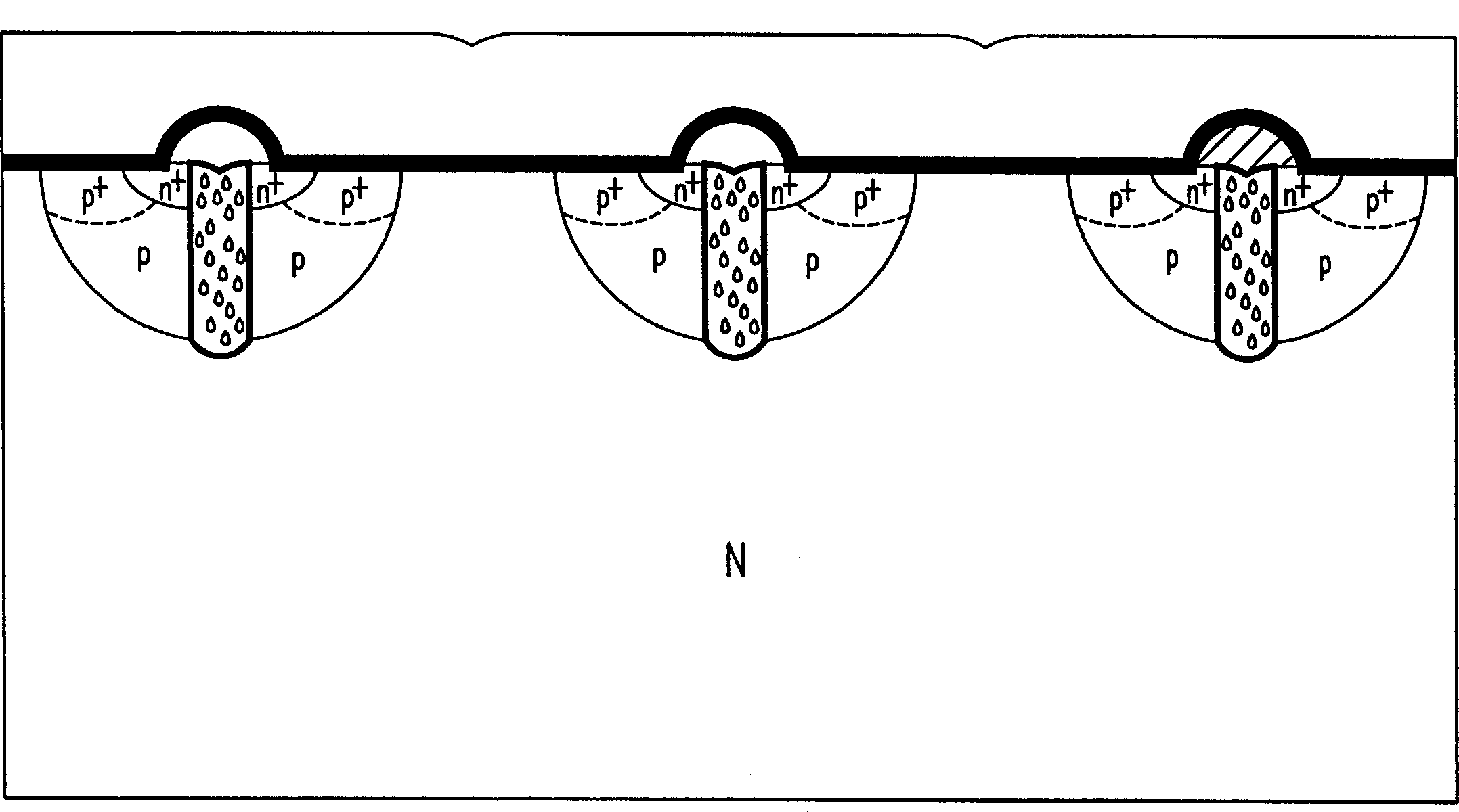
[0028] See Figure 6 It is a schematic diagram of the structure of a Schottky shielded diode (SBD) according to a preferred embodiment of the present invention. Such as Figure 6 As shown, the manufacturing method of the Schottky Shielded Diode (SBD) is to first form a plurality of groove structures 61 on the surface of a silicon wafer 60 by etching. Among them, the base material of the silicon wafer 60 is preferably silicon and silicon carbon base materials. After the top metal layer 62 (the uppermost layer of metal) is deposited, the shielding metal layer 63 of the Schottky Shielded Diode (SBD) can then be formed on the surface of the creped silicon wa...


PUM


Abstract

The present invention relates to a method to manufacture a schottky shielding diode, which forms a number of grooves on the base material and also forms a metal layer on the said base material which has a number of groove as well as forms a shielding metal layer between the base material and the metal layer in order to form the schoottky shielding diode.

Description

(1) Technical field [0001] The invention relates to a Schottky shielded diode and a manufacturing method thereof, in particular to a low forward voltage drop Schottky shielded diode and a manufacturing method thereof. (2) Background technology [0002] Recently, Schottky Barrier Diode (SBD) has been widely used in DC-DC converter (DC-DC converter), voltage regulator module (Voltage Regulator Module VRM), telecom transmission / server (Telecom) / Server), Adaptor and Charger, etc. See figure 1 , Which is a schematic diagram of an existing Schottky shielded diode. Such as figure 1 As shown, the manufacturing method of the Schottky shielded diode is to deposit a metal layer 11 on a silicon wafer 10, and the shielding metal 12 of the Schottky shielded diode (SBD) can then be generated on the silicon wafer 10. On the surface. The current transfer mode of the existing Schottky shielding diode is simulated as figure 2 Shown. [0003] In all these applications, Schottky shielded diodes (...

Claims


Application Information

Patent Timeline
Patent Type & Authority Applications(China)
IPC IPC(8): H01L21/329H01L29/872
Inventor 曾军周明江吴宗宪
Owner ONIZUKA ELECTRONICS
Why Eureka
Try Eureka