Semi-conductor manufacturing factory layout

A technology for manufacturing plants and semiconductors, which is applied in the field of configuration forms of semiconductor manufacturing plants, and can solve problems such as configuration forms that are difficult to solve

Inactive Publication Date: 2003-12-31
李珩铭
View PDF0 Cites 4 Cited by
  • Summary
  • Abstract
  • Description
  • Claims
  • Application Information

AI Technical Summary

Problems solved by technology

[0009] The purpose of the present invention is to provide a configuration form of a semiconductor manufacturing factory area, so as to contin

Method used


Image

  • Semi-conductor manufacturing factory layout
  • Semi-conductor manufacturing factory layout
  • Semi-conductor manufacturing factory layout

Examples


Embodiment Construction

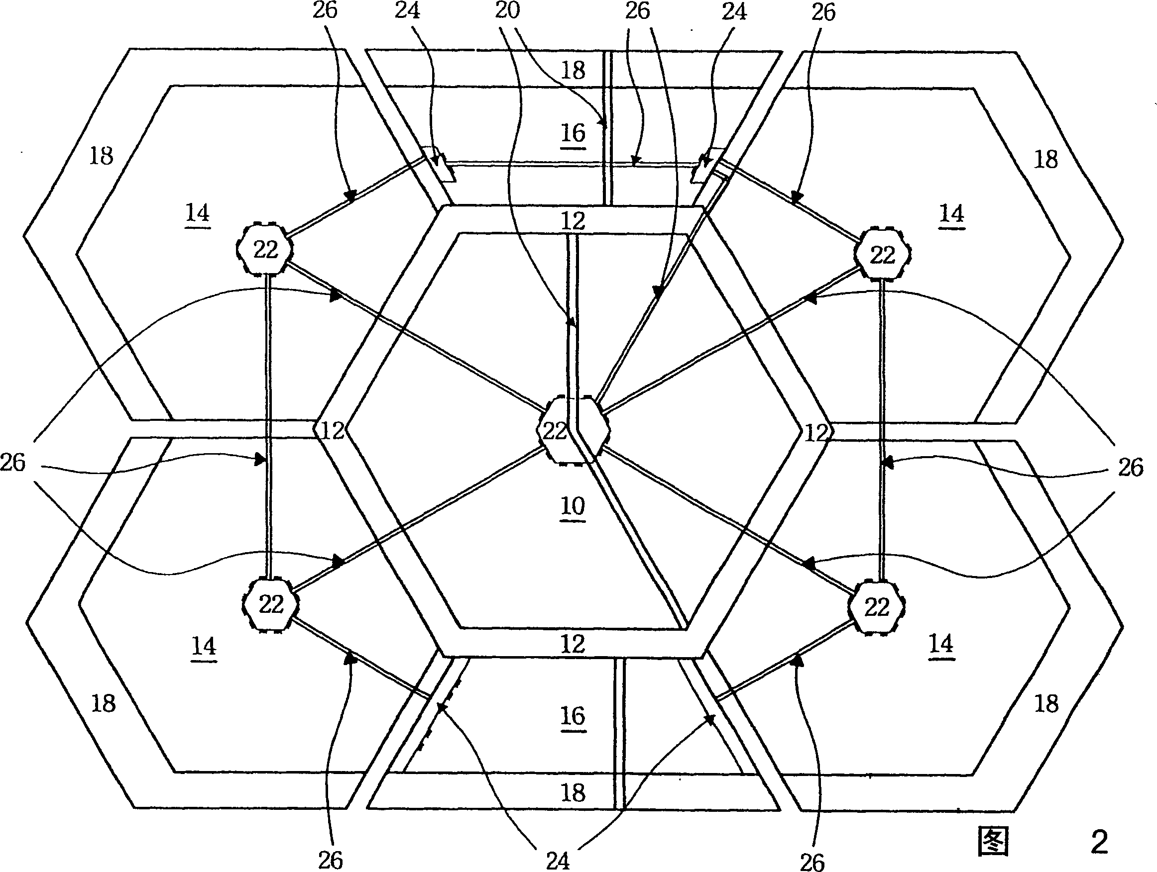
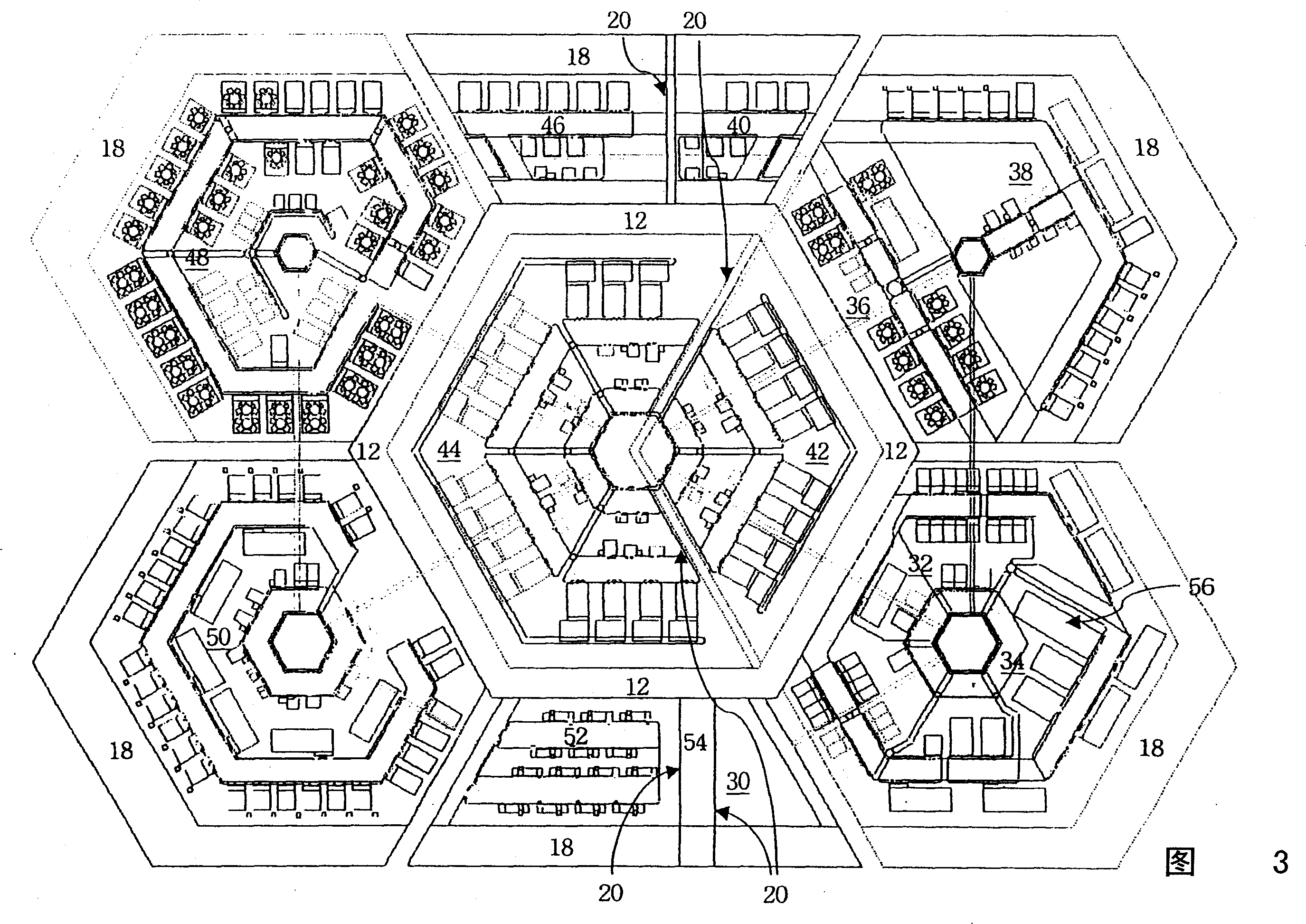
[0021] Referring to Fig. 2, the configuration form of the present invention can be divided into seven main areas, which are respectively a regular hexagonal area 10 in the center and four equiangular (120°) but not equilateral hexagonal areas around it. 14, and the upper and lower trapezoidal regions 16 (the inner angles are respectively 60°, 120°, 120°, and 60°) corresponding to adjacent hexagons. These seven main areas will provide the layout of the process areas in the semiconductor factory area, and each area can include more than one process area depending on the environmental characteristics of each process area, the relationship between logistics and the area requirements.

[0022] Continue to refer to Figure 2, the area of ​​the central regular hexagonal area 10 needs to meet the area requirements of the process area in this area, and the area is determined by the machine equipment, maintenance space, personnel operation and material handling in the process area in the ...


PUM


Abstract

The configuration mode for semiconductor factory workshops includes seven main areas including one central hexagonal area, four peripheral hexagonal areas to the right and left sides and two peripheral trapeziform areas in the other two sides. The manufacture workshop most closely relative to material circulation is set in the central area for the automatic material circulation in shortest path and highest efficiency. The configuration may be planned flexibly according to the required areas, environment and numbers of equipment in different workshops to raise the overall utilization of the factory area. The configuration is beneficial to concentrated management and control, simplified building construction, etc.

Description

(1) Technical field [0001] The present invention relates to the structure and form of the layout design of the semiconductor factory area, and in particular to the layout design of the process area in the semiconductor factory and the layout design of the machine equipment in the process area. (2) Background technology [0002] Generally speaking, the manufacture of semiconductor integrated circuit products needs to go through a series of hundreds of processing steps to complete, in which many machine tools with specific process functions are required. The relevant processes used by these machines and equipment need to be carried out in a specific environment, such as specific environmental factors such as cleanliness, temperature and humidity, light, and shock resistance, to ensure the stability and yield of products in the process. Therefore, the semiconductor factory must divide several process areas with considerable uniqueness in the environment and production character...

Claims


Application Information

Patent Timeline
IPC IPC(8): E04H5/02
Inventor 李珩铭
Owner 李珩铭
Why Eureka
Try Eureka