Si etching method and device

一种蚀刻装置、蚀刻的技术,应用在放电管、电气元件、半导体/固态器件制造等方向,能够解决处理效率低、蚀刻速度慢、不能高长宽比的槽蚀刻等问题

Inactive Publication Date: 2004-04-21
TOKYO ELECTRON LTD
View PDF0 Cites 13 Cited by
  • Summary
  • Abstract
  • Description
  • Claims
  • Application Information

AI Technical Summary

Problems solved by technology

[0005] Due to HBr / O 2 Mixed gas cannot etch high aspect ratio trenches, so it is not suitable for DTI
In addition, there are problems of slow etching speed, low processing efficiency, and low productivity.

Method used


Image

  • Si etching method and device
  • Si etching method and device
  • Si etching method and device

Examples


Embodiment 1~8

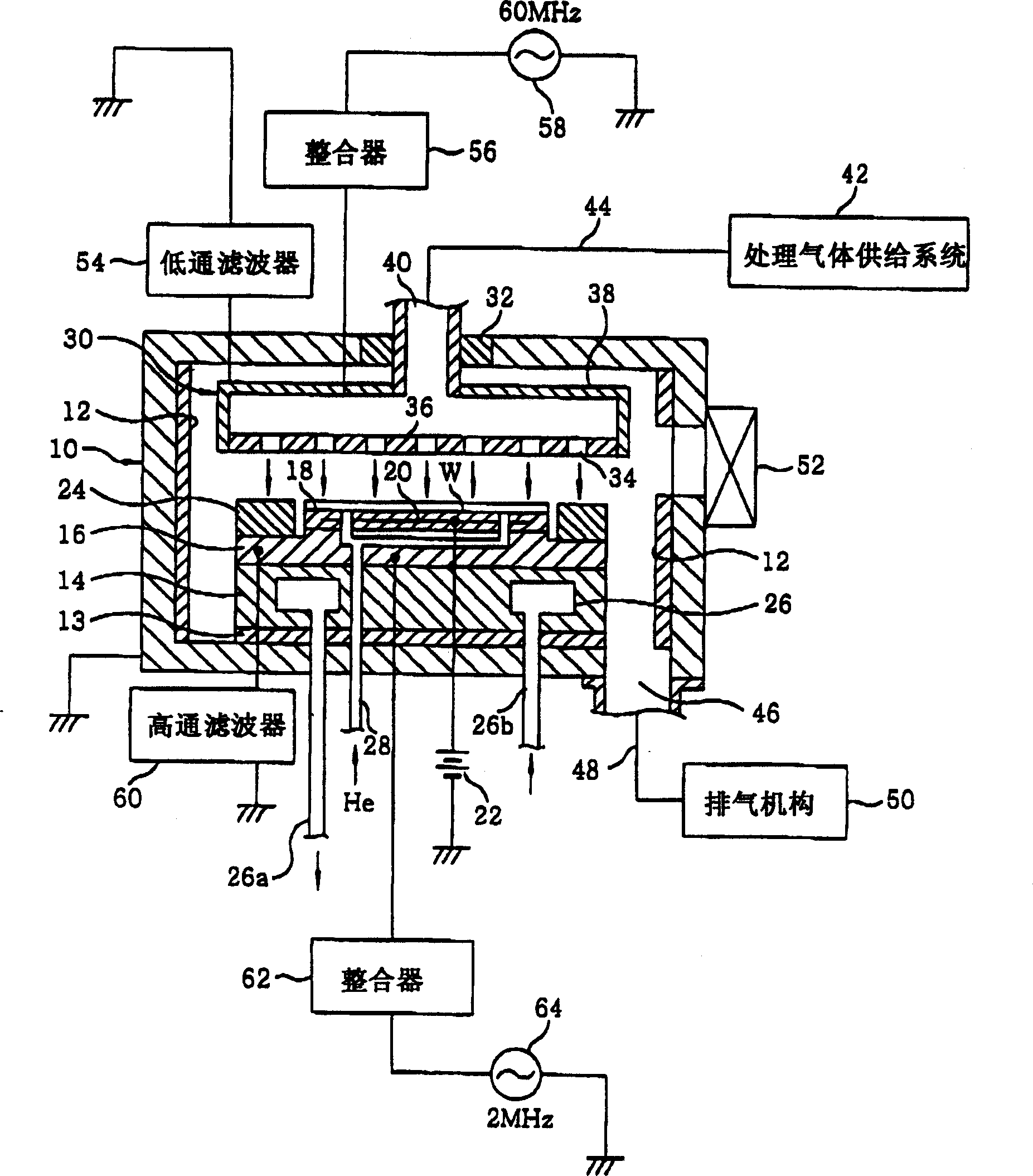
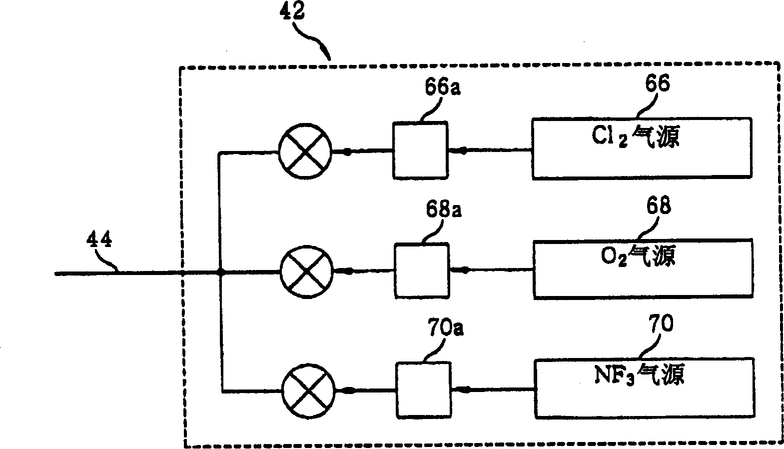
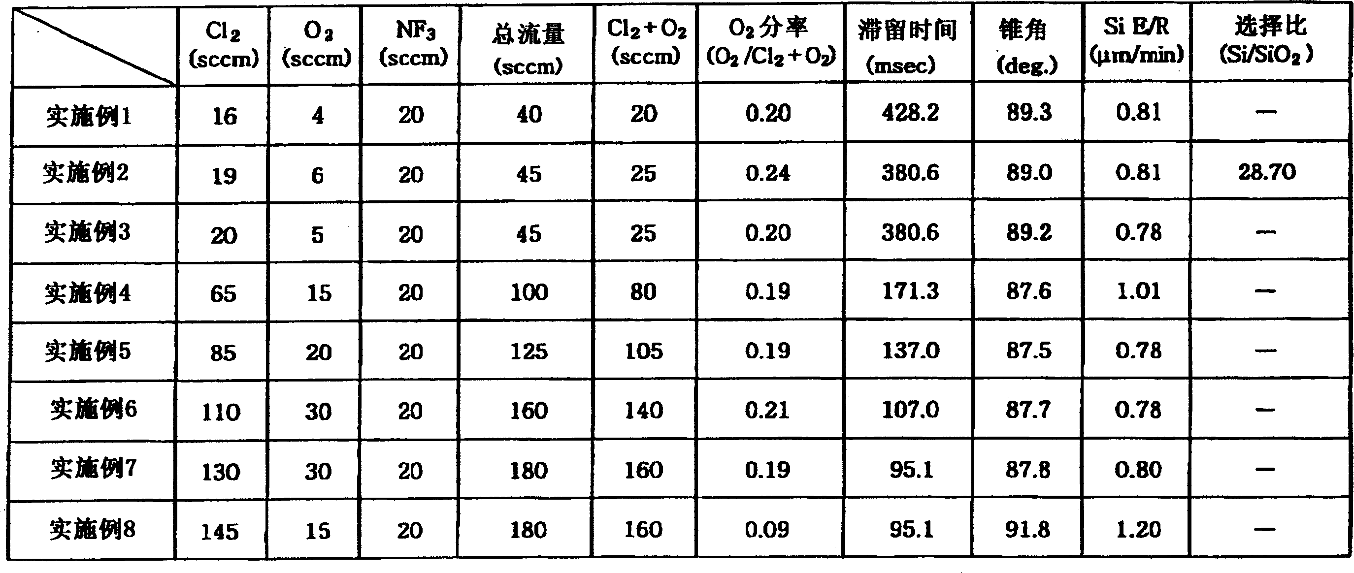
[0042] Used in the etching of grooves for DTI that form grooves with an opening width of 0.3 μm and a depth of 3 to 6 μm on Si wafers. figure 1 The plasma etching device, with etching gas (Cl 2 / O 2 / NF 3 ) flow rate and flow rate ratio are parameters to evaluate the characteristics of the etching gas. Other main etching conditions are as follows. image 3 and Figure 4 Data representing the results of an experiment.

[0043] Si wafer aperture: 200mm

[0044] Mask material: SiO 2 (upper layer) / SiN (lower layer) double film structure

[0045] Mask Thickness: (SiO 2 / SiN)=3000A / 1500A

[0046] Pressure: 60mTorr

[0047] RF power (upper electrode / lower electrode): 500W / 600W

[0048] Electrode spacing: 115mm

[0049] Temperature (upper electrode / lower electrode / chamber sidewall): 80 / 60 / 60°C


PUM


Abstract

To achieve a high aspect ratio and improvement of the etching rate in Si etching. Mixture gas of Cl2 / O2 / NF3is introduced from a process gas supply part 42 into a chamber 10 as an etching gas, and etching is performed under the condition, where the residence time is about 180 nsec or larger. High-frequency near 60 MHz is applied from a first high-frequency power source 58 to an upper electrode 30 at a specified power level. Further, a high frequency near 2MHz is applied from a second high-frequency power source 64 to a lower electrode (susceptor) 16 with a specified power level. The etching gas, discharged from a porous electrode plate or a shower head 36 of the upper electrode 30, is turned into a plasma during the glow discharge between the electrodes, and a Si wafer W is etched by radicals and ions generated in the plasma.

Description

technical field [0001] The invention relates to a technique for etching Si (silicon), in particular to an etching method and device suitable for forming and processing small-diameter deep trenches on Si substrates or Si layers. Background technique [0002] A trench separation method for separating elements in an LSI (Large Scale Integrated circuit) is generally an STI (Shallow Trench Isolation) method. In STI, a Si substrate is dry-etched using a resist layer or an insulating film as a mask to form relatively shallow grooves (grooves) with a depth of 1 μm or less. For this trench etching, a technique for controlling the depth and shape of the trench, especially the angle of the side wall (taper angle) is required. [0003] At present, STI uses etching gas, mostly using mixed gas with Br (bromine element) as the basic raw material, typically HBr / O 2 mixed composition. Since the HBr pairs pass O 2 The oxide film (SiO 2 ) is relatively weak in attack, so it is easy to be ...

Claims


Application Information

Patent Timeline
Patent Type & Authority Applications(China)
IPC IPC(8): H01L21/306H01L21/302H01L21/3065H01L21/461
CPCH01J37/32082H01L21/3065H01L21/306
Inventor 斋田喜孝山口雅司
Owner TOKYO ELECTRON LTD
Why Eureka
Try Eureka