

Semiconductor intergrated circuit device
A technology of integrated circuits and semiconductors, applied in the manufacture of semiconductor devices, circuits, semiconductor/solid-state devices, etc., can solve problems such as insufficient realization, and achieve the effect of area reduction
- Summary
- Abstract
- Description
- Claims
- Application Information
AI Technical Summary
Problems solved by technology
Method used
Image

Examples
Embodiment Construction
[0028] specific implementation
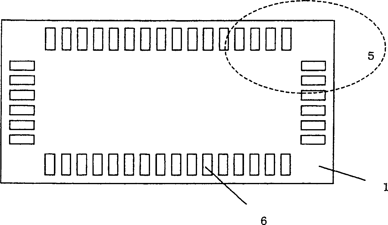
[0029] Below, refer to Figure 1 to Figure 6 Embodiments of the semiconductor integrated circuit device of the present invention will be described in detail.
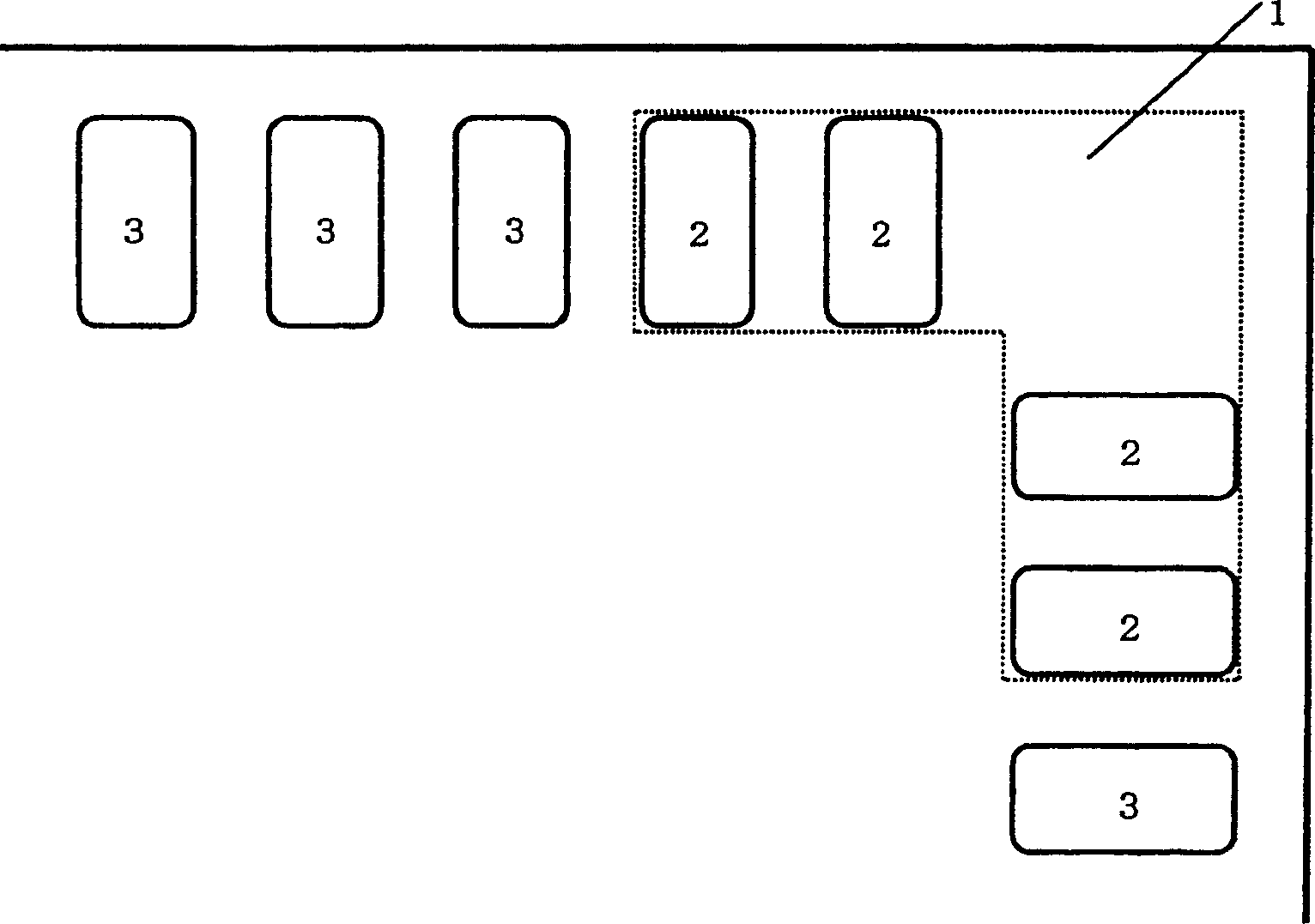
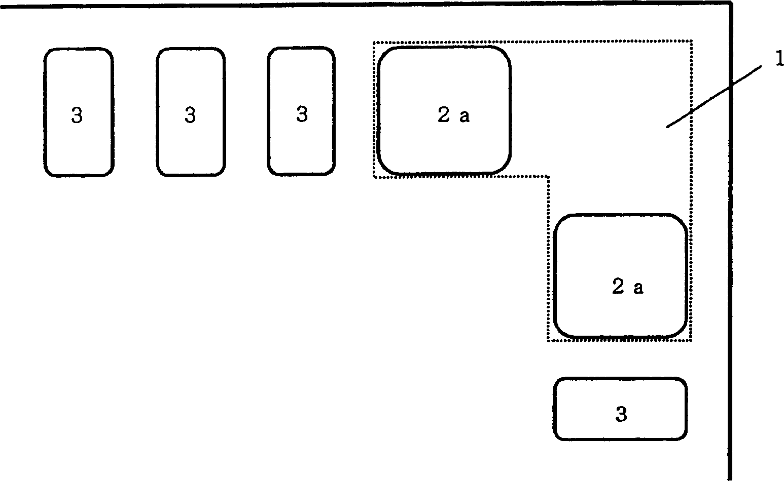
[0030] here, image 3 , Figure 4 , Figure 5 This is an enlarged view representing four corners of a chip corner of a semiconductor integrated circuit device chip. Each figure will be described below.
[0031] image 3 It is a bump arrangement diagram showing Example 1. It is provided with a bump 3 for circuit connection connected to an internal circuit not shown, and a dummy bump 2a is provided on each side of the part closer to the corner of the chip 1 of the semiconductor integrated circuit device. , and the area of the dummy bumps 2a is about twice the area of the bumps 3 for circuit connection, so a total load-bearing effect equivalent to the area of 4 bumps 3 for circuit connection is obtained. The inner portion of the portion shown by the dotted line is an area guar...
PUM
 Abstract
Description
Claims
Application Information