Semiconductor manufacturing system

A manufacturing system and semiconductor technology, applied in semiconductor/solid-state device manufacturing, gaseous chemical plating, coating, etc., can solve problems such as expensive processing costs, difficulty in loading and unloading semiconductor chips, and complex structure, so as to improve uniformity, Effect of preventing mechanical or physical defects and optimizing contact area

Inactive Publication Date: 2004-06-16
TERASEMICON CO LTD
View PDF0 Cites 11 Cited by
  • Summary
  • Abstract
  • Description
  • Claims
  • Application Information

AI Technical Summary

Problems solved by technology

However, semiconductor manufacturing systems with additional supporting devices are not only complex in structure, but also cannot avoid mechanical deformation in addition to expensive handling costs, and users also have difficulties in loading and unloading semiconductor wafers

Method used


Image

  • Semiconductor manufacturing system
  • Semiconductor manufacturing system
  • Semiconductor manufacturing system

Examples


Embodiment Construction

[0033] The present invention will be fully described below with reference to the accompanying drawings, in which the preferred embodiments of the present invention are shown. However, the present invention can be implemented in a variety of different forms and is not limited to the listed embodiments; and these embodiments are provided to fully and comprehensively disclose the present invention and convey the principles of the present invention to those skilled in the art.

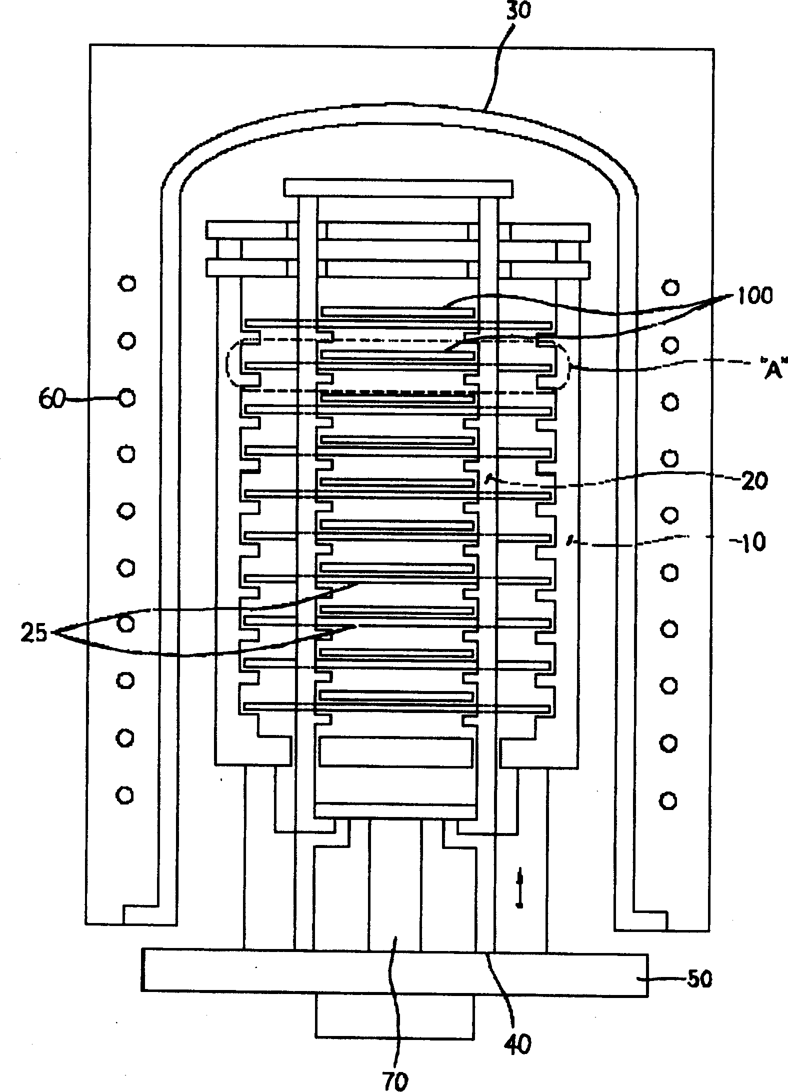
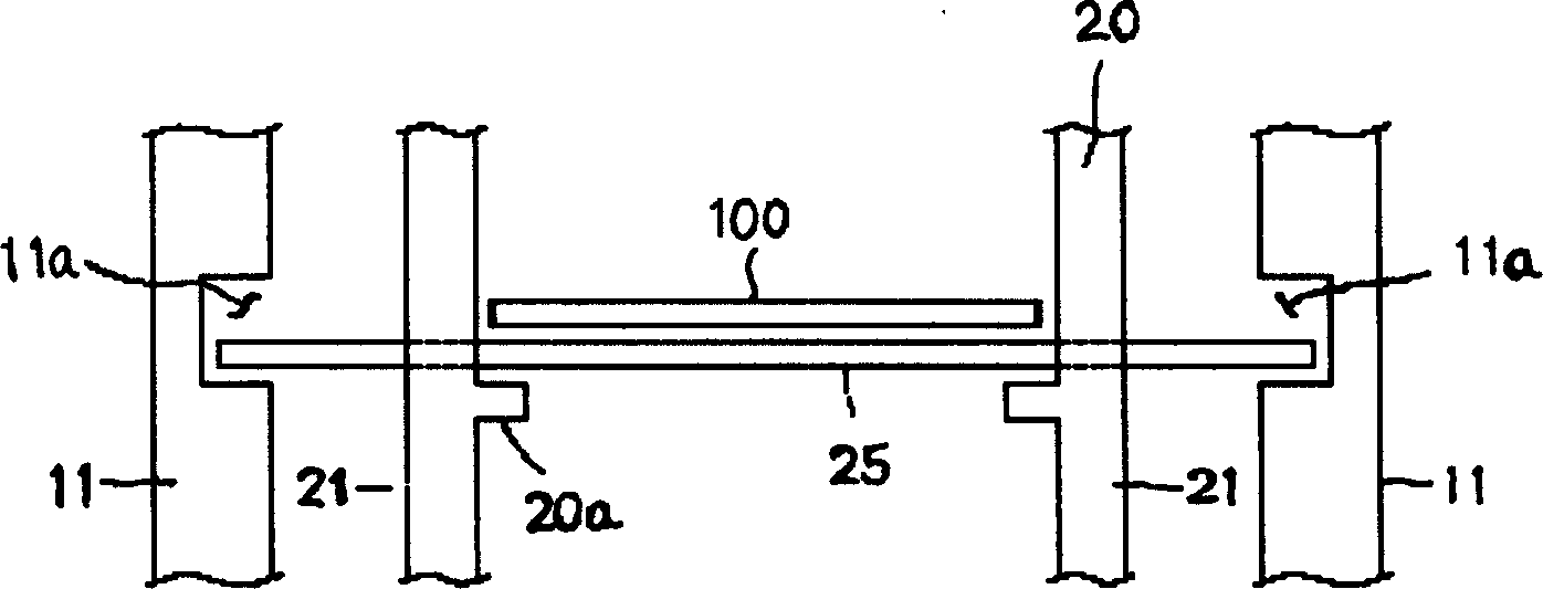
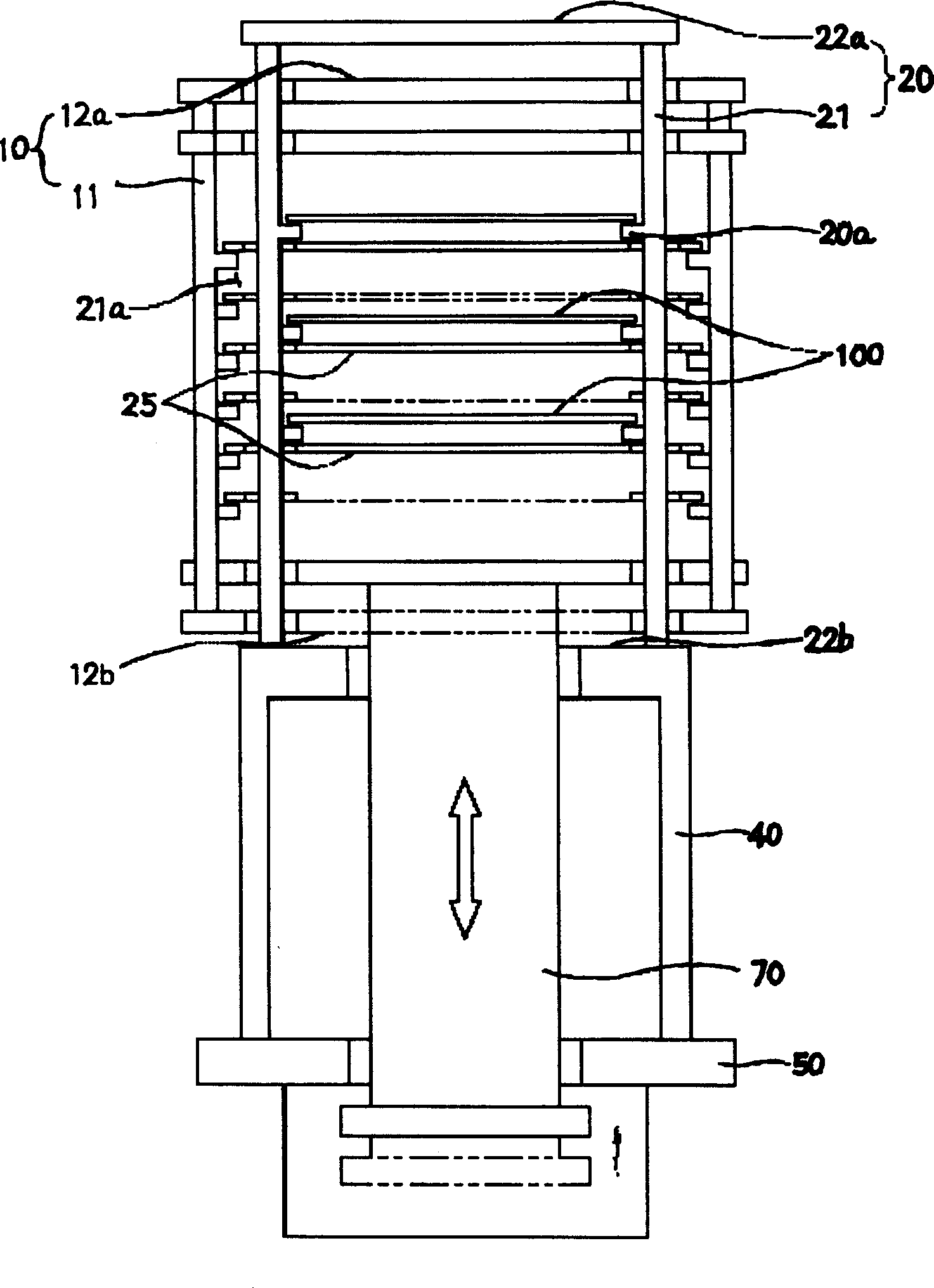
[0034] figure 1 It is a cross-sectional view of the semiconductor manufacturing system of the present invention. Figure 2 is figure 1 An enlarged cross-sectional view of part "A" in the middle. Figure 2B It is a cross-sectional view of a double vessel mounted in a semiconductor chip according to an embodiment of the present invention.

[0035] Reference figure 1 , The semiconductor manufacturing system includes a reaction tube 30 for heat treatment. The reaction tube 30 includes a double vessel, and the d...


PUM


Abstract

Semiconductor manufacturing system for loading semiconductor wafers into a vertical reaction tube and performing a thermal process has a first wafer loading boat mounted in the reaction tube and having holder supporters to support a wafer holder in a shape of a board, a second wafer loading boat having a wafer supporter, a plate cap, a door plate, and a lifting system which moves the wafer loading boat(s) vertically. Semiconductor manufacturing system capable of loading semiconductor wafers into a vertical reaction tube and performing a thermal process comprises a first wafer loading boat (10) which is mounted in the reaction tube and includes holder supporters that support a wafer holder (25) in a shape of a board, a second wafer loading boat (20) which is inside or outside the first wafer loading boat and has a wafer supporter that is located under the semiconductor wafer (100) to support the semiconductor wafer, a plate cap (40) which supports the first wafer loading boat and the second loading plate in their lower portions, a door plate (50) which supports the plate cap in the lower portion of the plate cap, and a lifting system (70) which moves at least one of the first wafer loading boat and the second wafer loading boat vertically and separates the semiconductor wafer, which is loaded on the wafer holder, from the wafer holder at a predetermined height during wafer load and unload cycles.

Description

Technical field [0001] The present invention relates to a semiconductor manufacturing system, in particular to the following semiconductor manufacturing system, which has a vertical reaction tube through which multiple semiconductor wafers can be processed at a time. Background technique [0002] Since a long-term heat treatment is required in the semiconductor manufacturing process, it is preferable to process a plurality of semiconductor wafers at the same time. In the semiconductor manufacturing system, the heat treatment process usually uses a slide vessel as a slide structure and a tube-shaped vertical reaction tube on which the semiconductor wafer is placed. This is because the uniformity of the heat treatment is affected by the uniformity of the flow of the reaction gas. influences. In the chip carrier, slots are formed at vertical intervals to support the semiconductor chip, and then at least one or two edges of the semiconductor chip are installed in the slot. [0003] H...

Claims


Application Information

Patent Timeline
Patent Type & Authority Applications(China)
IPC IPC(8): H01L21/683C23C16/458H01L21/22H01L21/324H01L21/673
CPCY10S206/832H01L21/67309H01L21/324
Inventor 朴承甲刘政昊
Owner TERASEMICON CO LTD
Why Eureka
Try Eureka