
Printed circuit board fabrication-related device

A printed circuit board, a specific technology, is applied in the direction of printed circuit manufacturing, printed circuit, printed circuit assembly of electrical components, etc., which can solve the problems of increased height and overall volume of the device, so as to achieve easy visual and operation, Suppresses the effect of excessive volume

Active Publication Date: 2004-06-16
CKD
View PDF0 Cites 1 Cited by
  • Summary
  • Abstract
  • Description
  • Claims
  • Application Information

AI Technical Summary

Problems solved by technology

[0005] However, when the display monitor is placed and fixed on the upper surface of the casing, the overall height of the device will increase, which will inevitably lead to an increase in the overall volume of the device.

Method used


Image

  • Printed circuit board fabrication-related device
  • Printed circuit board fabrication-related device
  • Printed circuit board fabrication-related device

Examples


Embodiment Construction

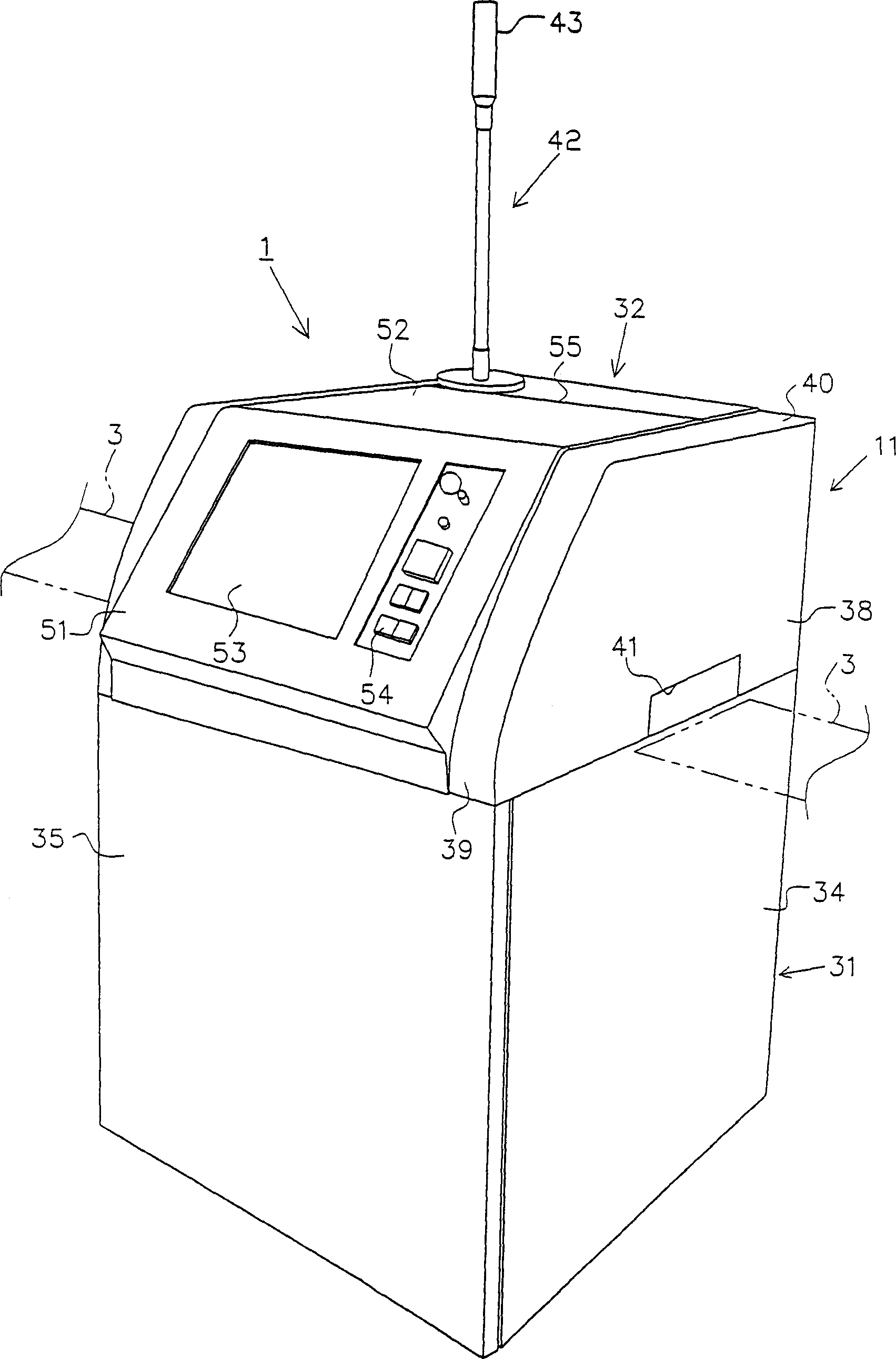
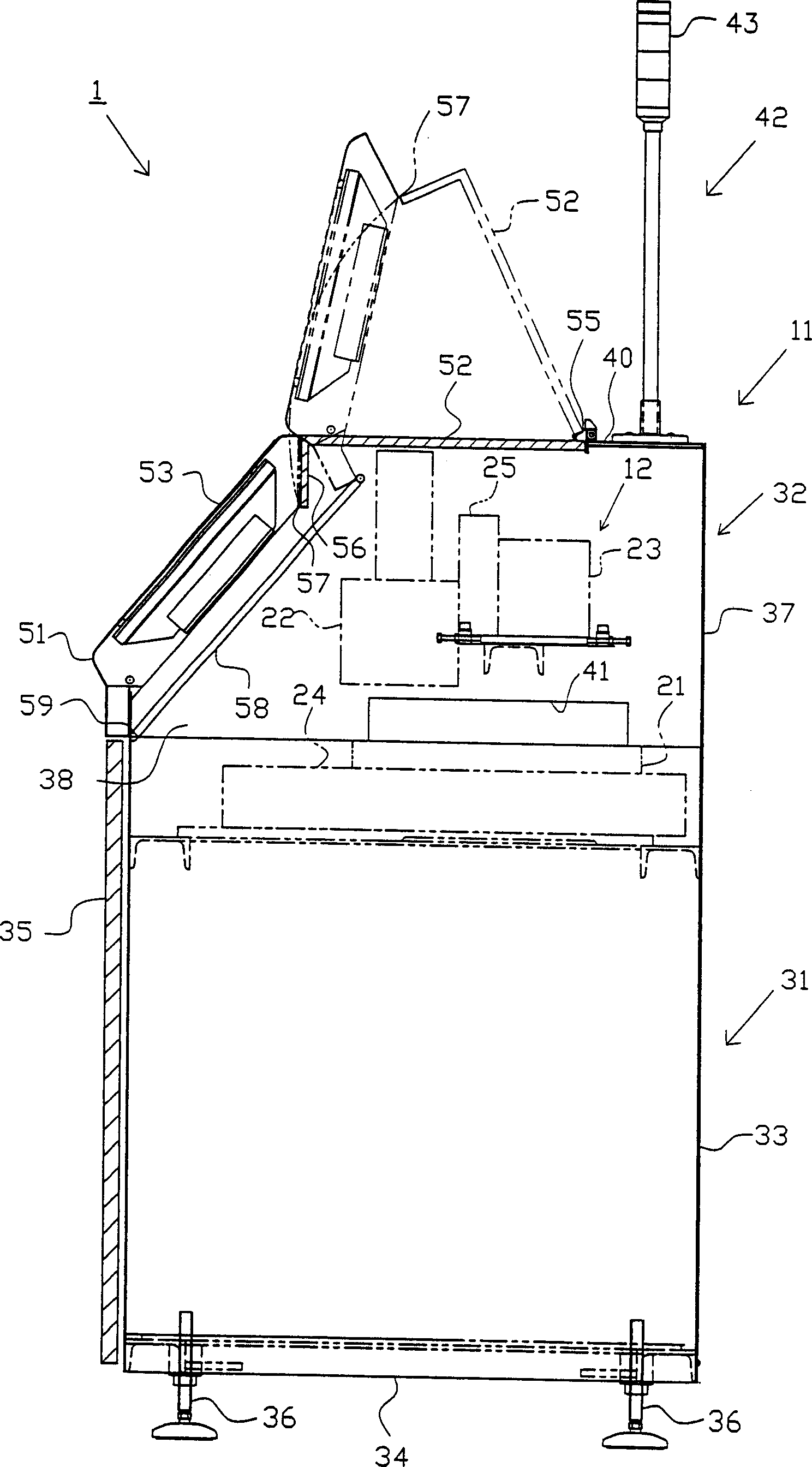
[0043] Next, an embodiment of the present invention will be described with reference to the drawings. In this embodiment, as an apparatus related to printed circuit board manufacturing, specifically, an inspection device 1 is used for inspecting a printed state of a printed circuit board (hereinafter, simply referred to as "circuit board") 2 on which solder is printed.

[0044] In a series of manufacturing processes, the circuit board 2 is conveyed to a predetermined height by the conveyor 3 from the left to the right of the figure. Here, the predetermined height refers to a height position at which an operator can easily perform work, and in this embodiment, it is set to a height position of 900 mm from the ground, for example. The detection device 1 is installed in the middle of the transport path of the conveyor 3 .

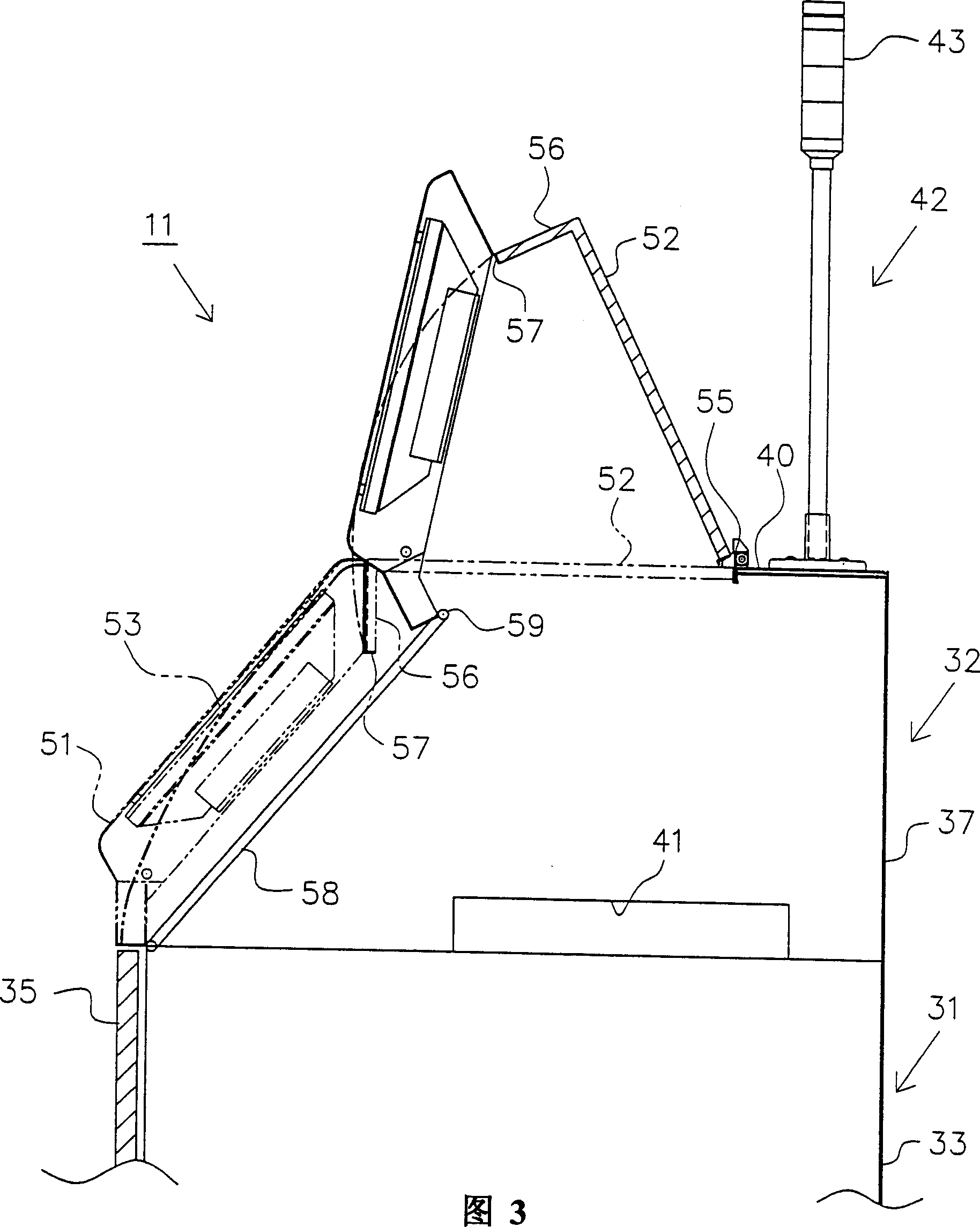
[0045] Such as figure 1 and figure 2 As shown, the detection device 1 has a housing 11 and a detection mechanism 12 installed in the housing 11 and actual...


PUM


Abstract

Provided is printed circuit board manufacturing related equipment which has improvement in the visibility of a display unit and can be suppressed the size increase. An inspection apparatus 1 comprises a housing 11 and an inspecting means installed inside the housing 11. The housing 11 comprises a lower case 31 and an upper case 32. The upper case 32 is fixed to the lower case 31, and comprises an upper rear wall 37, right and left upper side walls 38, a front wall 39 extended obliquely backward from on a front door 35, and a top wall 40 located on these walls 37, 38, and 39. The right and left upper side walls 38 are formed with openings 41 for passing a substrate through. For most of the front wall 39 and top wall 40 of the upper case 32, a lid structure which can be opened and closed is employed. Nearly in a central part of the upper case 32, a front lid 51 equipped with a liquid crystal touch panel 53 is so installed as to move upward.

Description

technical field [0001] The present invention relates to a printed circuit board manufacturing-related device used in a printed circuit board manufacturing process. Background technique [0002] In the manufacturing process of a printed circuit board, there exists a process of mounting an electronic component on a circuit board as a main process. When mounting an electronic component, first, cream solder is printed on a predetermined electrode pattern provided on a printed circuit board. Next, the electronic component is temporarily fixed on the printed circuit board according to the viscosity of the solder. Thereafter, the above-mentioned printed circuit board is introduced into a reflow furnace, undergoes a predetermined reflow process, and performs soldering. In such a series of work steps, the circuit board is conveyed in a predetermined direction on a conveyor positioned at a predetermined height (for example, the height of the operator's waist), and various operations...

Claims


Application Information

Patent Timeline
Patent Type & Authority Applications(China)
IPC IPC(8): H05K3/34G01R31/00H05K3/00
Inventor 多贺僚治高桥国夫
Owner CKD
Learn More