Drive device for semiconductor storage device, and method for operating drive device

A storage device and driver technology, applied in semiconductor devices, static memory, electric solid-state devices, etc., can solve the problems of increased number of contacts, increased cost, increased number of pins, etc.

Inactive Publication Date: 2004-07-28
INFINEON TECH AG
View PDF0 Cites 0 Cited by
  • Summary
  • Abstract
  • Description
  • Claims
  • Application Information

AI Technical Summary

Problems solved by technology

[0004] In addition, the output current I for fast switching on and off at a high transfer rate out Voltage induction will be formed at both ends of the inductance of the feeder, especially the grounding inductance connected to the grounding network of the drive. In order to keep this useless induced voltage as low as possible, a large number of parallel feeders or grounding connections are often used to reduce the lower than A preset limit of overall inductance to ground, which would lead to an increase in the number of pins on the package or an increase in the number of contacts, resulting in an increase in the cost of packaging and encapsulation

Method used


Image

  • Drive device for semiconductor storage device, and method for operating drive device
  • Drive device for semiconductor storage device, and method for operating drive device
  • Drive device for semiconductor storage device, and method for operating drive device

Examples


Embodiment Construction

[0051] In the diagram, the downward pointing connection point and the end point of the arrow represent connection to a ground network or potential.

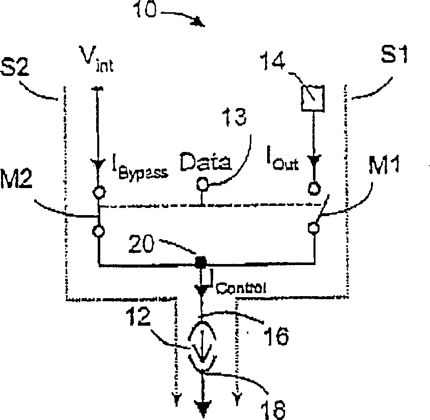
[0052] In the follow-up content, please refer to FIG. 3(A) to FIG. 5 for the driver device 10 of the first preferred embodiment of the present case.

[0053] The driver device 10 is preferably operated in open-drain mode, with or without on-chip termination resistors.

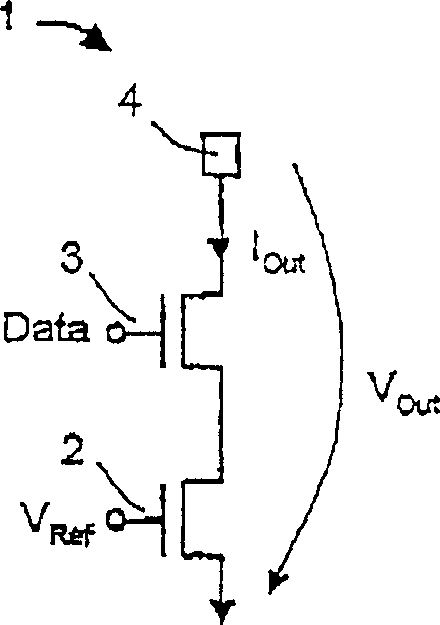
[0054] Fig. 3 (A) is the circuit diagram of the driver device 10 of a first preferred embodiment of the present case, wherein the driver device 10 forms a semiconductor storage device (especially a main memory of a computer) or an integrated circuit (not shown) In part, the driver device 10 is used to convert a (voltage) signal from or to the semiconductor storage device into a (current) signal and amplify it.

[0055] The driver device 10 includes a current control device 12, a first switching device M1, and a second switching device M2 for providing an internal...


PUM


Abstract

The driver contains current control with the two contacts, driver input contact for input data and driver output contact, dependent on output data. Between driver output contact and first current control contact lies first current path with first switch for interruption first current path flow in dependence on driver input data. Second current path is coupled to first current control contact and contains second switch for interrupting second current path flow. Both switches safeguard interruption of first or second current path. Independent claims are included for semiconductor memory with invented driver and for operational method of driver.

Description

technical field [0001] This case relates to a current-mode drive device for a semiconductor storage device, in particular to a semiconductor storage device and a method for operating the drive device. Background technique [0002] Known driver devices for semiconductor storage devices are used to generate, for example, an amplified output signal, figure 1 shows one possible circuit configuration of an output driver 1 in current mode mode, the output driver 1 comprising REF "A transistor 2, in addition, it also includes a second transistor 3 connected in series with the gate electrode, used to transmit a data signal (voltage signal) "data", the output signal generated is output through the driver output contact 4, in In the case of an output driver of the current mode type, the output signal is I out A selected output current, and in the present case, two different output signal values ​​are divided by the current I out Flow through or not flow through the driver output co...

Claims


Application Information

Patent Timeline
IPC IPC(8): G11C7/10
CPCG11C7/1057G11C7/1051
Inventor G·布劳恩
Owner INFINEON TECH AG
Why Eureka
Try Eureka