Supercharge Your Innovation With Domain-Expert AI Agents!

Electronic device with wide lens and for small firing point size

An electronic device and lens technology, applied in the field of microelectronics, can solve the problems of poor quality of the tip of the emitter, complicated process, low yield, etc.

Inactive Publication Date: 2004-08-04
HEWLETT PACKARD DEV CO LP
View PDF0 Cites 0 Cited by
  • Summary
  • Abstract
  • Description
  • Claims
  • Application Information

AI Technical Summary

Problems solved by technology

These create process complications as it is difficult to deposit a tip emitter in a deep well without coating the interior of the well when forming the emitter tip
This may require more complex tools such as larger evaporators
Deep wells can also cause poor emitter tip quality and low yield

Method used


Image

  • Electronic device with wide lens and for small firing point size
  • Electronic device with wide lens and for small firing point size
  • Electronic device with wide lens and for small firing point size

Examples


Embodiment Construction

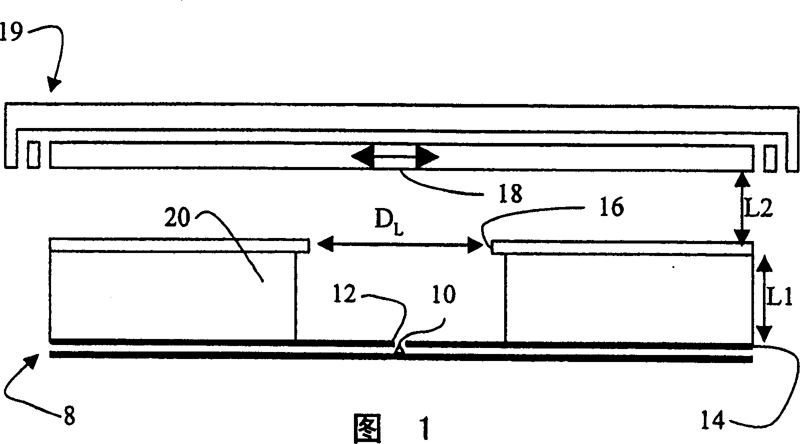
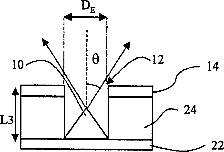
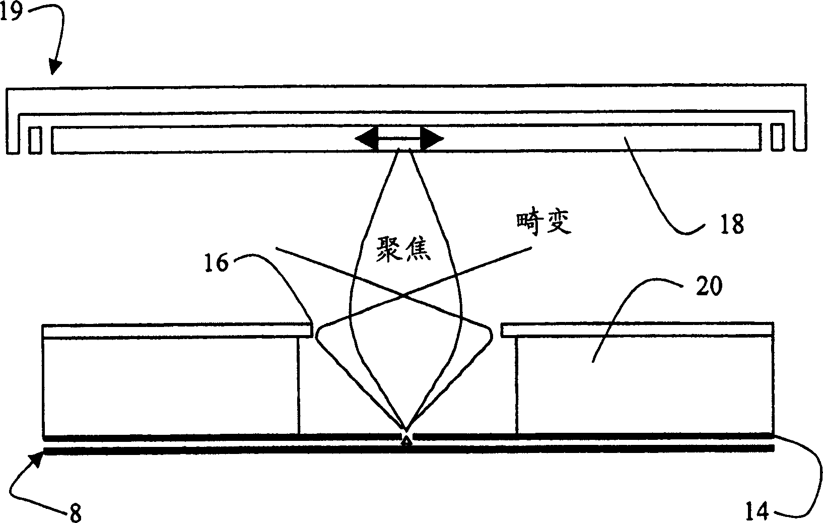
[0024] The electronic device of the present invention will be implemented using a focusing lens formed as a structure on the extractor of the emitter device after formation of the emitter device. The lens is made significantly wider than the extractor to enclose the diverging electrons, the lens is also placed at a considerable distance from the extractor to extend the flight path of the electrons compared to conventional arrangements, and allows a single lens to obtain small focus spot size. In some embodiments, no aperture is used. In an alternative embodiment, an aperture is used at the extractor to further reduce the spot size. The use of a separately formed focusing lens according to the present invention allows the relative size of the lenses to be determined independently of the size of the extractor / tip well, which can be placed at a desired distance from the extractor, e.g. form on the dielectric thereby moving it away from the extractor. When the emitter and its w...


PUM


Abstract

An electronic device includes a tip emitter (10) formed in a well (12) that is defined in a substrate (8). An extractor (14) disposed about the well extracts emissions from the tip emitter (10). A wide lens (16) focuses the emissions through its opening. The opening is sufficiently large and spaced far enough away to encompass the majority of a divergence angle of the emissions. The emissions are focused into a spot.

Description

technical field [0001] The present invention is in the field of microelectronics and in particular relates to devices utilizing focused emission from emitters. Background technique [0002] Computing technology will continue to become cheaper while computing technology provides higher performance, and physical size has shrunk to meet the purpose of portability, especially in portable devices that need to provide a portable power source such as a battery. Power loss must be minimized . [0003] The high power requirements of traditional memory devices such as hard drives limit the long-term operation of batteries. Microprocessors consume a small amount of power compared to these auxiliary devices, even in higher speed devices. There are complaints in the trade press that mass storage devices, such as disk drives, CD-ROMs, DVD drives to name a few, cannot keep up with the speed of microprocessor development. [0004] Electron emitters that generate electron beams provide the...

Claims


Application Information

Patent Timeline
Patent Type & Authority Applications(China)
IPC IPC(8): H01J37/073G11C7/00H01J1/30H01J1/304H01J3/02H01J37/305H01L21/027
CPCG11C7/005H01J2237/31754H01J3/021H01J1/30
Inventor P·本宁H·-P·霩W·R·奈特P·H·麦克莱兰德
Owner HEWLETT PACKARD DEV CO LP
Features
  • R&D
  • Intellectual Property
  • Life Sciences
  • Materials
  • Tech Scout
  • Unparalleled Data Quality
  • Higher Quality Content
  • 60% Fewer Hallucinations
Learn More